
Timeline
Timeline
2026-02-17
init
This article introduces the basics of LCD (Liquid Crystal Display) in Linux driver notes. It first outlines the working principle of LCD, that is, the molecular arrangement of liquid crystals changes under an electric field, affecting its optical properties, and compares the technical differences between CRT displays and OLED screens. It then elaborates on the characteristics and application scenarios of five mainstream LCD panel technologies: TFT, TN, IPS, VA, and SLCD, and compares IPS, VA, and TN panels in terms of color, response time, viewing angle, and contrast ratio. Finally, it explains the concept of pixels, stating that any color can be mixed by controlling the brightness of red, green, and blue, laying the foundation for subsequent understanding of LCD driver development.
Linux Driver Notes
| Table of Contents | Links |
|---|---|
| 1. Linux Driver Framework | |
| 2. Linux Driver Loading Logic | |
| 3. Character Device Basics | |
| 4. Concurrency and Race Conditions | |
| 5. Advanced Character Device Topics | |
| 6. Interrupts | |
| 7. Platform Bus | |
| 8. Device Tree | |
| 9. Device Model | |
| 10. Hotplug | |
| 11. pinctrl Subsystem | |
| 12. GPIO subsystem | |
| 13. Input subsystem | |
| 14. 1-Wire | |
| 15. I2C | |
| 16. SPI | |
| 17. UART | |
| 18. PWM | |
| 19. RTC | |
| 20. Watchdog | |
| 21. CAN | |
| 22. Network devices | |
| 23. ADC | |
| 24. IIO | |
| 25. USB | |
| 26. LCD |

LCD Introduction
LCD Overview
LCD stands for Liquid Crystal Display, i.e., a liquid crystal display.
Liquid crystal is a special substance between solid and liquid. Under the action of an electric field, the arrangement of liquid crystal molecules changes, thereby affecting its optical properties.
LCD is also one of the commonly used peripherals. It can display images and interfaces, and combined with touch and a mouse, it can also enable human-computer interaction. For instance, LCD is found in most everyday computer screens and mobile phone screens.
Before LCD monitors became widespread, CRT monitors were the mainstream display devices, commonly known as “big-head” monitors.
This type of display is rarely seen today. The full name of CRT is “Cathode Ray Tube”, and it uses cathode ray tube technology to display images.
A CRT display mainly consists of five key components:
- An electron gun for emitting electron beams
- Deflection coils that control the direction of the electron beam
- A shadow mask for precisely focusing the electron beam
- Graphite electrodes that provide high-voltage support
- And a phosphor layer coated on the inner wall of the screen and a glass shell.
These components work together to convert electronic signals into visible images.
In addition to LCD, more advanced OLED screens have emerged today. For example, many flagship phones currently use OLED screens.
OLED stands for “Organic Light-Emitting Diode”, and its display principle is different from traditional LCD:
OLED does not require a backlight; instead, it uses a very thin organic material coating and a glass substrate (or flexible substrate). When current passes through, these organic materials emit light on their own.
LCD Panels
LCD can be subdivided into TFT, TN, IPS, VA, and SLCD, which represent different liquid crystal panel technologies. Each technology has its own unique characteristics and application scenarios. The specific description of each technology is as follows:
| Technology Name | Full name | Description |
|---|---|---|
| TFT | Thin Film Transistor | TFT displays are the mainstream display devices in various laptops and desktops. Each liquid crystal pixel is driven by a thin film transistor integrated behind the pixel, so it is an active-matrix liquid crystal display device. TFT displays have advantages such as high responsiveness, high brightness, and high contrast, and their display quality is close to that of CRT monitors, making them one of the high-end products among LCD color displays. |
| TN | Twisted Nematic | TN panels are entry-level liquid crystal panels. Due to their low production cost, they are widely used in mid-to-low-end LCD monitors. Although their performance is relatively basic, their low cost makes them one of the mainstream choices in the market. |
| IPS | In-Plane Switching (IPS) display technology | IPS technology, developed by Hitachi in 1996, is a wide-viewing-angle liquid crystal display technology. Compared with TN screens, IPS can effectively improve the color shift problem that occurs at poor viewing angles, and is widely used in the manufacture of LCD TVs and tablet computers, providing better display quality. |
| VA | Vertical Alignment (VA) | VA panels are a liquid crystal panel technology that balances the advantages of TN and IPS, offering high contrast and good color performance at a moderate price. Its disadvantage is slower response time, and it is commonly used in mid-to-high-end monitors and scenarios with certain image quality requirements, such as home theater displays. |
| SLCD | Splice Liquid Crystal Display (SLCD) | SLCD is a high-end derivative of LCD, using industrial-grade LCD panels with a service life of up to 60,000 hours. It can be used alone as a monitor or spliced into an ultra-large screen. It is a complete splicing display unit, suitable for high-end display scenarios. |
IPS, VA, and TN panels each have their own advantages and disadvantages.
- In terms of color and color accuracy, IPS performs best, followed by VA, and TN last;
- In terms of response time, TN panels are the fastest, IPS is second, and VA is the slowest;
- In terms of viewing angles, IPS performs best, VA is second, and TN is the worst;
- In terms of contrast ratio, VA panels are the strongest, IPS is in the middle, and TN is the weakest.
Overall, different panel types have their own characteristics across various indicators, and you can choose the appropriate panel according to your needs.
Pixel
Using the control principles of liquid crystals, it is possible to design display structures that can adjust the output intensity of the three colors red, green, and blue. Combining these three display structures into one display unit, and by precisely controlling the brightness of each color, the unit can display different colors. Such a display unit is called a ‘pixel’.
Therefore, a pixel can be compared to a small RGB light, and since RGB are the three primary colors of light, they can be mixed to produce any color.
Resolution
If a screen has a resolution of 1920x1080, then there are 1920x1080=2,073,600 pixels in total. So resolution is the number of pixels that make up the screen.
Generally speaking, the higher the resolution, the better the display effect, but resolution is not the only criterion. Screen brightness, color accuracy, and viewing angle are also important parameters that affect the display quality.

For example, in the image above, the horizontal axis is X and the vertical axis is Y. If it represents a 1920x1080 resolution screen, there are 1920 pixels in the X direction and 1080 pixels in the Y direction. It can be seen that the higher the resolution, the better the display effect. It is an important parameter for measuring screen display quality.
Pixel Format
A pixel is similar to a small RGB light, and RGB are the three primary colors of light that can form any color. So by controlling the brightness of the three RGB colors, any color can be displayed. So how do we control the brightness of the three RGB colors?
The three RGB colors generally use 8-bit data each, so one pixel is 8 bits x 3 = 24 bits. This pixel format is called RGB888. It can displaycolors.
In addition to the RGB888 pixel format, there are also RGB565, RGB666, etc. That is:
- RGB565: R-5bit, G-6bit, B-5bit, can displaycolors.
- RGB555: R-5bit, G-5bit, B-5bit, can displaycolors.
So, is it better to choose a screen with a larger pixel format?
Suppose there is a screen with a resolution of 1920x1080. If a 24-bit pixel format is used, the required bandwidth is 1920x1080x24, but if a 16-bit pixel format is used, the required bandwidth is 1920x1080x16. It can be seen that:
**The larger the pixel format, the greater the required bandwidth.**Therefore, when choosing a pixel format, it is limited by factors such as interface bandwidth and processor capability.
PPI
PPI is pixel density, which stands for Pixels Per Inch, indicating the number of pixels per inch. The PPI calculation formula is as follows:
From the calculation formula, it can be seen that when calculating screen PPI, the diagonal length in inches is used as the measurement.
For example, a 10-inch screen with a resolution of 2400x1080 has a calculated PPI of 263, while a screen with the same resolution but 8 inches in size has a calculated PPI of 329, so the latter naturally has better display detail.
LCD Interface Types
There are many types of LCD interfaces. Common ones in embedded systems include RGB, MIPI, LVDS, and EDP interfaces, while common ones on monitors include DP, HDMI, VGA, etc. A brief introduction to each interface is as follows:
| Interface Name | Introduction |
|---|---|
| RGB | Parallel digital interface, uses TTL levels to transmit red, green, and blue signals, commonly used in early LCD screens and embedded displays. |
| MIPI | High-speed serial digital interface, designed specifically for mobile devices (such as phones/tablets), uses differential signal transmission, features low power consumption and supports high resolution. |
| LVDS | Low-voltage differential serial digital interface, strong anti-interference capability, widely used in mid-to-high-end screens such as laptops and monitors. |
| EDP | Embedded DisplayPort interface, based on high-speed serial digital transmission, with a rate far exceeding LVDS, suitable for high-resolution laptops, tablets, and professional monitors. |
| VGA | Analog signal interface, transmits via RGBHV signals, strong compatibility but limited resolution, gradually being replaced by digital interfaces. |
| HDMI | Fully digital audio/video interface, supports high resolution and synchronized audio transmission, widely used in TVs, monitors, and consumer electronic devices. |
DBI, DPI, and DSI Interface Categories
DBI, DPI, and DSI interfaces are another classification of screen interfaces by DWG (Display Working Group), a working group of the MIPI Alliance. They do not conflict with the RGB, MIPI, LVDS, EDP, etc. interfaces mentioned above.
The DBI interface is also called the MCU interface or 8080 interface, with the full name Display Bus Interface. It can transmit control commands and data through a parallel interface, and refresh the screen by updating data in the GRAM built into the LCD module.
DPI stands for Display Pixel Interface, which is a parallel interface. For example, the RGB interface mentioned earlier can be classified as a DPI interface.
DSI stands for Display Serial Interface, which is a serial display interface and an image output interface defined by the MIPI Alliance.
LCD Touch Screen Composition
In embedded development, commonly used LCD screens mostly have touch functionality, enabling human-machine interaction through touch operations. It should be noted that the LCD and the touch screen are two independent components, each serving different functions. The LCD screen is mainly responsible for displaying images and content, while the touch part focuses on detecting user touch input and implementing interactive control.
The LCD screen part is shown below:

LCD touch component:

Some LCDs are a single piece, not composed of two parts as described above. This is because the LCD and the touch layer are bonded together to form a module that can both display content and support touch operations.
Depending on the bonding method, common processes are divided into two types: full lamination and frame bonding:
- Full lamination is commonly used in consumer products, with the advantage of a thinner module;
- Frame bonding, on the other hand, is mostly used in industrial scenarios, offering higher reliability and durability.
LCD screens usually need to be paired with a screen adapter board for connection to the development board. Note that in the embedded field, there is no unified standard for LCD screen interfaces, and pin orders may differ between manufacturers. Therefore, when connecting a screen, be sure to carefully verify the pin order to avoid the risk of damaging the screen, development board, or core board due to mismatched pin order.
Display Controller
Basic Concepts of Display Controller
The display controller, also known as LCDC (full name: LCD Controller), is mainly responsible for transferring image data in memory to display devices.
With the continuous development of technology, the functions of display controllers have also been enhanced, enabling them to handle some simple image operations such as scaling, rotation, and image composition.
The role of the display controller in a processor is similar to that of a graphics card in a computer. When a processor integrates a display controller, it is equivalent to having a built-in graphics card module that can directly drive the display to output image signals.
For example, high-performance SoCs such as RK3399, RK3588, and RK3568 all have built-in display controllers, enabling video output without additional hardware.
The framework diagram of a processor with an integrated display controller is shown below:

In the embedded field, some low-power microcontrollers (such as the STM32 series) usually do not integrate a display controller. If such processors need to achieve image output, they must connect an external display module with GRAM to complete graphics processing and display functions.
Framework diagram of a processor without an integrated display controller:
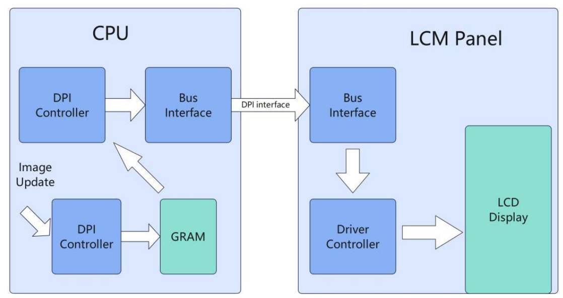
Processor architectures without an integrated display controller typically have the following characteristics:
- Limited graphics processing capability, relying on the computing resources provided by an external display module.
- System power consumption and hardware cost are relatively low, making it suitable for scenarios with high requirements for energy efficiency and economy.
- Mainly used in fields with basic display requirements such as industrial control and sensor panels.
VOP Introduction
In Rockchip’s series of SoCs, the display controller is called VOP (Video Output Processor). Currently, there are two VOP architectures in Rockchip processors: VOP1 and VOP2.
The difference between the two is mainly reflected in the way multi-screen display is supported. Typically, one VOP can only drive one screen for independent display at a time. To achieve multi-screen display, multiple VOPs need to work together.
VOP1
VOP1 uses this traditional approach to support multi-screen display (one VOP can only drive one screen for independent display at a time). The functional diagram of the VOP1 architecture is shown below:

For example, the display controller built into the RK3399 processor is of type VOP1. The description of VOP in the RK3399 processor’s TRM manual is as follows:
In the RK3399 processor, two VOP modules are integrated, named VOP_BIG and VOP_LIT. Therefore, the RK3399 can support up to two screens displaying simultaneously.
VOP2
In contrast, the VOP2 architecture contains only one VOP module in the processor, but multiple independent VP (Video Port) output interfaces are designed at its backend. These VP interfaces can work independently at the same time, thereby achieving multiple display outputs. That is,The display capability of VOP2 depends on the number of VPs, with as many VPs as there are, it can support that many simultaneous displays (same display or different displays). The functional diagram of the VOP2 architecture is shown below:

Taking the RK3568 processor as an example, its Technical Reference Manual (TRM) describes VOP2 as follows:

VOP2 is a display interface module that connects the memory frame buffer to the display device. It connects to the AHB bus via the AHB Slave interface for register configuration; at the same time, it connects to the AXI bus via the AXI Master interface for reading display frame data.
Therefore, for the RK3568 processor, it supports up to 3 screens with same or different display. Each VP of the RK3568 processor also supports LCD screens with different interfaces. As shown in the figure below:

Among them, VP0 and VP1 both support output to MIPI0, MIPI1, eDP, and HDMI interfaces, while VP2 supports output to LVDS and RGB interfaces. This diverse interface configuration enables the RK3568 to adapt to a variety of display devices, fully reflecting its flexibility in LCD interface design.
It should be noted that each VP can only support output to one display interface at a time. For example, if VP1 is configured for LVDS output, it cannot be used for HDMI output at the same time. In addition, the maximum resolution capabilities of different VP interfaces also vary. The maximum resolution support for each VP interface is detailed as follows:
| VOP Channel | Maximum Resolution @ Refresh Rate | Supported Interfaces and Corresponding Resolution @ Refresh Rate |
|---|---|---|
| VP0 | 4096×2304@60Hz | - HDMI: 4096×2160@60Hz - eDP: 2560×1600@60Hz - MIPI: 1920×1080@60Hz (Single-channel) - MIPI: 2048×1536@60Hz (Dual-channel) |
| VP1 | 1920×1080@60Hz | - HDMI: 1920×1080@60Hz - eDP: 1920×1080@60Hz - MIPI: 1920×1080@60Hz (Single-channel) - LVDS: 1280×800@60Hz |
| VP2 | 1920×1080@60Hz | - LVDS: 1280×800@60Hz - RGB: 1920×1080@60Hz |
Connector-mirror technology
In the RK3568 chip, there are three independent video processing units (VP), so under the most basic conditions, the RK3568 supports three display outputs. If more simultaneous outputs are needed, this can be extended by using connector-mirror technology.
For example, the RK3588, based on four VOPs combined with connector-mirror technology, can achieve an application scenario with seven simultaneous display output signals.

The figure above uses connector-mirror technology to connect two HDMI/eDP outputs to VP0, two DP outputs to VP1, two MIPI DSI outputs to VP2, and VP3 outputs via BT656 and BT1120, thus achieving seven simultaneous outputs.
With the above configuration, the system can output up to 7 display signals simultaneously, but these signals are actually implemented through 4 independent display paths. It should be noted that,The display timing and content output by each group (i.e., the two display interfaces on the same Video Port) are exactly the same.。
In this application mode, the maximum resolution of each display path**is limited by the maximum resolution supported by the corresponding Video Port and the connected display interfaces.**This feature can be enabled through DTS (Device Tree Source) configuration. In the DTS file, simply mount the two display interfaces under the same Video Port to complete the configuration.
Currently, this feature is only supported in the NVR SDK, while Android does not support it for now.
VOP-Split technology
The VOP-Split function is a technology similar to MIPI dual-channel mode. It can split the output of one Video Port horizontally into left and right parts, thereby driving two display interfaces simultaneously. In this mode, the display timing of the two display interfaces remains consistent, but they can output independent images.
It should be noted that this feature is currently only supported on hardware platforms based on the VOP2 architecture. By using the VOP-Split function, more efficient display expansion capabilities can be achieved. The application block diagram for expansion using the VOP-Split function is shown below:
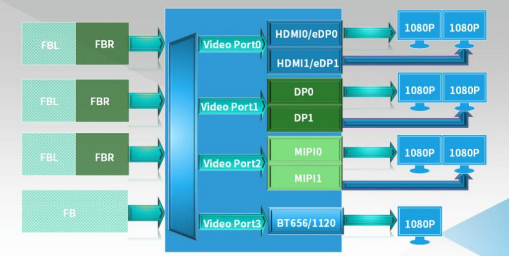
After enabling Split mode on VP0, the output of VP0 can drive two display interfaces simultaneously (e.g., HDMI0/1, eDP0/1, or other display interfaces connected to VP0). The content presented on these two display interfaces is the result of dividing the VP0 output image horizontally into left and right halves.
For example, if VP0 outputs at a resolution of 3840x1080, each display interface will display a 1920x1080 image.
It should be noted that in Split mode, the two display interfaces participating in output on the same VP must maintain the same display timing and frame rate.
Glossary
| Term | Explanation |
|---|---|
| Encoder | An encoder that converts the image signal output by the display controller into a digital signal, such as HDMI, MIPI, etc. |
| Connector | A connector that transmits the signal output by the encoder to a display and establishes a connection with the display. |
| Bridge | A bridge device, generally referring to a conversion chip, such as RGB to HDMI. |
| Panel | Generally refers to a specific display screen. |
| Plane | Layer. The output image is composed of multiple layers overlaid, such as a primary layer, cursor layer, etc. |
| GEM | The full name is generic DRM memory-management, which manages the video memory used by DRM, including dumb, prime, and fence. |
| Framebuffer | Framebuffer is a cache (memory) abstracted by Linux from video memory. Its purpose is to provide a set of interfaces at the application layer to directly operate the screen, without needing to care about details such as the physical video memory location and paging mechanism. The Framebuffer device file is generally/dev/fb*。 |
LCD timing
Glossary
| Signal | Full name | Function |
|---|---|---|
| HSYNC | Horizontal Sync | Controls the horizontal scan synchronization signal to ensure each row of pixels is correctly aligned. |
| HPW | Horizontal Low Pulse Width | Defines the electronic pulse width of the horizontal sync signal. |
| HSA | Horizontal Sync Active | Indicates the time period during which the horizontal sync signal is in an active state. |
| HSS | Horizontal Sync Start | Indicates the start position of the horizontal sync signal. |
| HSE | Horizontal Sync End | Indicates the end position of the horizontal sync signal. |
| HBP | Horizontal Back Porch | The blank interval between the end of the horizontal sync signal and the start of the active pixel area. |
| HFP | Horizontal Front Porch | The blank interval between the end of the active pixel area and the start of the next horizontal sync signal. |
| HACT | Horizontal Active | Defines the width of the active pixel area in the horizontal direction of the screen. |
| VSYNC | Vertical Sync | Controls the vertical scan synchronization signal to ensure each frame is correctly aligned. |
| VPW | Vertical Low Pulse Width | Defines the low-level pulse width of the vertical sync signal. |
| VSA | Vertical Sync Active | Indicates the time period during which the vertical sync signal is in an active state. |
| VSS | Vertical Sync Start | Indicates the start position of the vertical sync signal. |
| VSE | Vertical Sync End | Indicates the end position of the vertical sync signal. |
| VBP | Vertical Back Porch | The blank interval between the end of the vertical sync signal and the start of the active pixel area. |
| VACT | Vertical Active | Defines the height of the active pixel area in the vertical direction of the screen. |
| VFP | Vertical Front Porch | The blank interval between the end of the active pixel area and the start of the next vertical sync signal. |
In some materials, some terms also have other names:
| Full name | Other names |
|---|---|
| HBP (Horizontal Back Porch) | left_margin |
| HFP (Horizontal Front Porch) | right_margin |
| VBP (Vertical Back Porch) | upper_margin |
| VFP (Vertical Front Porch) | lower_margin |
| HPW (HSYNC pulse width) | hsync_len |
| VPW (VSYNC pulse width) | vsync_len |
Timing
In Linux, the time parameters of the LCD, i.e., the timing, are abstracted. In the kernel source code:Documentation/fb/framebuffer.rstyou can find the abstract diagram of Linux’s LCD timing, as shown in the figure below
12345678910111213141516171819202122232425262728293031323334 | +----------+---------------------------------------------+----------+-------+| | ↑ | | || | |upper_margin | | || | ↓ | | |+----------###############################################----------+-------+| # ↑ # | || # | # | || # | # | || # | # | || left # | # right | hsync || margin # | xres # margin | len ||<-------->#<---------------+--------------------------->#<-------->|<----->|| # | # | || # | # | || # | # | || # |yres # | || # | # | || # | # | || # | # | || # | # | || # | # | || # | # | || # | # | || # | # | || # ↓ # | |+----------###############################################----------+-------+| | ↑ | | || | |lower_margin | | || | ↓ | | |+----------+---------------------------------------------+----------+-------+| | ↑ | | || | |vsync_len | | || | ↓ | | |+----------+---------------------------------------------+----------+-------+ |
The figure shows a physical device in which the “electron gun” draws each pixel row by row, pixel by pixel, in order from left to right and top to bottom. The entire frame is not fully presented until the last pixel has been drawn. This process is illustrated in the figure below:

The process by which the “electron gun” draws a frame is accomplished by scanning line by line in a zigzag pattern. Each line is drawn from left to right, and upon completion, it returns to the start of the next line, until the entire frame has been drawn.
In this process:
- HSYNC (horizontal sync signal) is used to indicate the start of drawing a new line, so it appears at the far right of each line;
- VSYNC (vertical sync signal) indicates the start of a new frame and appears at the bottom of the entire frame.
- In the abstract diagram, the Hactive and Vactive areas represent the actual image display area, while the surrounding HFP (Horizontal Front Porch), HBP (Horizontal Back Porch), VFP (Vertical Front Porch), and VBP (Vertical Back Porch) together form the so-called “black border”. Their existence is to allow time for signal switching and electron gun retrace.
The detailed explanation is as follows:
- HFP (Horizontal Front Porch): After the current line has been drawn, the electron gun is turned off, and this is the time before the next HSYNC signal is generated.
- HSYNC: Indicates the start of horizontal retrace, and the electron gun jumps back to the beginning of the next line.
- HBP (Horizontal Back Porch): The waiting time from the end of the HSYNC signal until the electron gun is turned on again to begin drawing a new line.
- VFP (Vertical Front Porch): After the entire frame has been drawn, the electron gun is turned off, and this is the time before the VSYNC signal is generated.
- VSYNC: Indicates the start of vertical retrace, and the electron gun returns to the top-left corner of the screen to prepare for drawing a new frame.
- VBP (Vertical Back Porch): The waiting time from the end of the VSYNC signal until the electron gun is turned on again to begin drawing a new frame.
Although these “black border” areas do not participate in actual image display, they are crucial for maintaining image stability and synchronization. The abstract diagram is shown below:

The “electron gun” is common in CRT monitors, but CRT monitors have now been phased out. There is no “electron gun” in LCDs. Instead, a chip is used to replace the “electron gun” to control the timing of the LCD.
LCD timing example
Here, the LCD timing diagram in the 4412 processor datasheet is used as an example for parameter analysis.

HSYNC: Horizontal scanning sync signal, also called line sync signal. The generation of this signal indicates the start of scanning a new line. In the figure above, the HSYNC signal is active high.
HSPW: HSYNC signal width. In some LCD datasheets, it is also called thp.
HBP/HBPD: The time from the end of the HSYNC signal to the start of the next valid data. Some LCD datasheets also call it thb, and some engineers also call it the back porch of the line sync signal, or the back swing of the line sync signal.
HFP/HFPD: The waiting time from the end of one line of valid data to the generation of the HSYNC signal. Some LCD datasheets also call it thf, and some engineers also call it the front porch of the line sync signal, or the front swing of the line sync signal.
VCLK: Pixel clock, also called PCLK. The frequency of the pixel clock signal is related to the resolution of the LCD. The higher the resolution, the higher the frequency of the pixel clock signal.
VDEN: Data enable signal, also called DE signal, indicates valid data. In the figure above, it is active high.
HOZVAL: Indicates the time required to scan one line. Some LCD datasheets also call it thd.
VSYNC: Vertical scan synchronization signal, also called frame synchronization signal. This signal indicates the start of displaying a new frame. In the figure above, the HSYNC signal is active high.
VSPW: VSYNC signal width, some LCD datasheets also call it tvp. VBP/VBPD: The time from the end of the VSYNC signal to the start of a new frame. Some LCD datasheets also call it tvb, and some engineers also call it the frame/vertical sync signal back porch, or the frame/vertical sync signal back swing.
VFP/VFPD: The time from the end of scanning one frame to the generation of the VSYNC signal. Some LCD datasheets also call it tvf, and some engineers also call it the frame/vertical sync signal front porch, or the frame/vertical sync signal front swing.
FRAME: The time required to display one frame.
When lighting up the screen, we need to determine the values of these parameters. We can refer to the screen’s datasheet or confirm them through the screen supplier’s FAE personnel. The following is a description of these parameters in an LCD screen datasheet.
| Item | Symbol | Min. | Typ. | Max. | Unit | Remark |
|---|---|---|---|---|---|---|
| Horizontal Display Area | thd | - | 1024 | - | DCLK | |
| DCLK Frequency | fclk | 40.8 | 51.2 | 67.2 | MHz | |
| One Horizontal Line | th | 1114 | 1344 | 1400 | DCLK | |
| HS pulse width | thpw | 1 | - | 40 | DCLK | |
| HS Blanking | thb | 160 | 160 | 160 | DCLK | |
| HS Front Porch | thfp | 16 | 160 | 216 | DCLK | |
| Vertical Display Area | tvd | - | 600 | - | TH | |
| VS period time | tv | 624 | 635 | 750 | TH | |
| VS pulse width | tvpw | 1 | - | 20 | TH | |
| VS Blanking | tvb | 23 | 23 | 23 | TH | |
| VS Front Porch | tvfp | 1 | 12 | 127 | TH |
RGB Screen Porting
RGB Interface Introduction
The iTOP-RK3568 core board supports the RGB interface and can connect to LCDs with an RGB interface. Note that the RGB interface is multiplexed into other functions on the baseboard.
The RGB interface resources of the iTOP-RK3568 core board and their multiplexed functions on the baseboard are as follows:
| RGB Signal | Corresponding GPIO | Net label | Baseboard Multiplexed Function |
|---|---|---|---|
| LCDC_D0 | GPIO2_D0_d | PCIE20_CLKREQn_M1 | PCIE2.0 Reference Clock Request |
| LCDC_D1 | GPIO2_D1_d | PCIE20_WAKEn_M1 | PCIE2.0 wake-up |
| LCDC_D2 | GPIO2_D2_d | PCIE30X1_CLKREQn_M1/SPI0_CS0_M1 | PCIE3.0 Reference Clock Request / SPI0 CS0 Pin |
| LCDC_D3 | GPIO2_D3_d | PCIE30X1_WAKEn_M1/SPI0_CLK_M1 | PCIE3.0 Wake-up / SPI CLK Pin |
| LCDC_D4 | GPIO2_D4_d | PCIE30X2_CLKREQn_M1 | PCIE3.0 Reference Clock Request |
| LCDC_D5 | GPIO2_D5_d | PCIE30X2_WAKEn_M1 | PCIE3.0 Wake-up |
| LCDC_D6 | GPIO2_D6_d | PCIE30X2_PERSTn_M1 | PCIE3.0 Reset |
| LCDC_D7 | GPIO2_D7_d | PCIE30X2_PRSNT_L_GPIO2_D7 | PCIE3.0 Insertion Detection |
| LCDC_CLK | GPIO3_A0_d | PCIE30X1_PRSNT_L_GPIO3_A0/PCIE20_PRSNT_L_GPIO3_A0 | PCIE3.0 Insertion Detection / PCIE2.0 Reset |
| LCDC_D8 | GPIO3_A1_d | PCIE30X1_PERSTn_M1 | PCIE3.0 Reset |
| LCDC_D9 | GPIO3_A2_d | I2S3_MCLK_M0 | I2S3 MCLK Pin |
| LCDC_D10 | GPIO3_A3_d | I2S3_SCLK_M0 | I2S3 SCLK Pin |
| LCDC_D11 | GPIO3_A4_d | I2S3_LRCK_M0 | I2S3 LRCK Pin |
| LCDC_D12 | GPIO3_A5_d | I2S3_SDO_M0/TP_INT_L_GPIO3_A5 | I2S3 SDO pin / Touch INT pin |
| LCDC_D13 | GPIO3_A6_d | I2S3_SDI_M0/USB_OTG_PWREN_H_GPIO3_A6 | I2S3 SDI pin / USB OTG power enable pin |
| LCDC_D14 | GPIO3_A7_d | GMAC1_INT/PMEB_GPIO3_A7 | GMAC1 INT and PMEB functions |
| LCDC_D15 | GPIO3_B0_d | GMAC1_RSTn_GPIO3_B0 | GMAC1 reset pin |
| LCDC_D16 | GPIO3_B1_d | UART4_RX_M1 | UART4 RX pin |
| LCDC_D17 | GPIO3_B2_d | UART4_TX_M1 | UART4 TX pin |
| LCDC_D18 | GPIO3_B3_d | I2C5_SCL_M0 | I2C5 SCL pin |
| LCDC_D19 | GPIO3_B4_d | I2C5_SDA_M0 | I2C5 SDA pin |
| LCDC_D20 | GPIO3_B5_d | RS485_DIR_GPIO3_B5 | RS485 input/output control pin |
| LCDC_D21 | GPIO3_B6_d | GPIO3_B6_d | GPIO3_B6 pin |
| LCDC_D22 | GPIO3_B7_d | GPIO3_B7_d | GPIO3_B7 pin |
| LCDC_D23 | GPIO3_C0_d | GPIO3_C0_d | GPIO3_C0 pin |
| LCDC_HSYNC | GPIO3_C1_d | PCIE20_PERSTn_M1 | PCIE2.0 reset |
| LCDC_VSYNC | GPIO3_C2_d | HP_DET_L_GPIO3_C2 | Headphone plug detection pin |
| LCDC_DEN | GPIO3_C3_d | SPK_CTL_H_GPIO3_C3/5G_RESET | Amplifier control pin / 5G reset pin |
The RGB interface typically requires 28 signal lines, which also explains why in baseboard designs, the RGB signal pins are often multiplexed for other functions. The reason is that once all RGB interface pins are brought out, they occupy 28 pins, resulting in excessive resource consumption.
Among these 28 signal lines, 24 are used to transmit color data, corresponding to the three color signals red ®, green (G), and blue (B). The specific signal lines are LCD_D0 ~ LCD_D23. The other 4 are control signal lines, including the horizontal sync signal (LCDC_HSYNC), vertical sync signal (LCDC_VSYNC), data enable signal (LCDC_DEN) and pixel clock signal (LCDC_CLK). The specific allocation is shown in the following table:
| Signal line | Function |
|---|---|
| R[7:0] | Red color data line |
| G[7:0] | Green color data line |
| B[7:0] | Blue color data line |
| LCDC_HSYNC | Horizontal synchronization data line |
| LCDC_VSYNC | Vertical synchronization data line |
| LCDC_DEN | Data enable data line |
| LCDC_CLK | Pixel clock data line |
In the RGB interface, the 24 color pins correspond to the three colors R, G, and B respectively, and the corresponding signal lines are LCD_D0~LCD_D23. Among these 24 color pins, R corresponds to 8 pins, G corresponds to 8 pins, and B corresponds to 8 pins. Taking the iTOP-RK3568 core board as an example, the official Rockchip documentation describes it as follows:

In the RGB interface, the connection method of the signal lines depends on the color format used.
For RGB888 format:
- The core board’s
D0 ~ D7correspond to the blue channelB0 ~ B7 D8 ~ D15correspond to the green channelG0 ~ G7D16 ~ D23correspond to the red channelR0 ~ R7。
- The core board’s
In RGB666 format:
- The lower two bits of the blue, green, and red channels (
B0 ~ B1、G0 ~ G1、R0 ~R1) are not connected, and the remaining signal lines are still connected according to the RGB888 mapping rules.
- The lower two bits of the blue, green, and red channels (
For RGB565 format:
- The low-order bits of the blue, green, and red channels (
B0 ~ B2、G0 ~ G1、R0 ~ R2) are not connected, and the remaining signal lines are also connected according to the RGB888 mapping rules.
- The low-order bits of the blue, green, and red channels (
This flexible connection method can adapt to different color format requirements while optimizing the use of pin resources.
Sync Mode
From the previous LCD timing analysis, it can be seen that the horizontal timing includes HFP (Horizontal Front Porch), HBP (Horizontal Back Porch), and HSYNC (Horizontal Sync Signal), while the vertical timing includes VFP (Vertical Front Porch), VBP (Vertical Back Porch), and VSYNC (Vertical Sync Signal).
These timing portions do not contain displayable data, so a mechanism is needed between the LCD and the processor to achieve synchronization.
The core function of synchronization isto enable the LCD to recognize the signal state currently sent by the processor, for example, when sending non-display timing such as HFP, the LCD will not display it as valid data; or notify the LCD that from a certain point in time, the subsequently transmitted data is valid display data and can be used for screen display.
To achieve this synchronization purpose, there are currently two main methods:
- DE mode
- HV mode
DE mode
Use the DE data line to indicate the start and end of valid data, for example, the LCDC_DEN signal line.

When the DE signal goes high, it indicates the start of valid data; when the DE signal goes low, it indicates the end of valid data. Therefore, in DE mode, signal lines such as HSYNC and VSYNC are not needed. It is relatively simple to use.
HV mode
In HV mode, the timing of the LCD needs to be determined by HSYNC (horizontal sync signal) and VSYNC (vertical sync signal), without using the DE (data enable) signal line. The synchronization work is completely accomplished by the HSYNC and VSYNC signals.

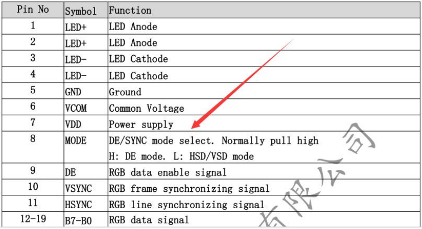
Currently, most LCD screens support both HV mode and DE mode. For example, the following screen is compatible with both modes and selects the specific working mode through its 8th pin:
When the 8th pin is at a high level, the screen operates in DE mode;
When the 8th pin is at a low level, it switches to HV mode.
This design provides developers with greater flexibility to choose the appropriate synchronization method according to actual needs.
Hardware schematic analysis
The iTOP-RK3568 core board itself brings out the RGB interface, but in the standard baseboard, this interface has been multiplexed for other functions. Therefore, if you need to use the RGB display function, you need to design and manufacture a compatible baseboard yourself.
The following takes the ‘iTOP-RK3568 core board + Topeet 5-inch RGB screen’ as an example. When designing the baseboard, you can refer to the schematic provided below for drawing and connection.

| Function | Pin number | Function | Pin number |
|---|---|---|---|
| LCDC_D0 | SPI0_MISO_M1 | LCDC_D14 | GMAC1_INT/PMEB_GPIO3_A7 |
| LCDC_D1 | SPI0_MOSI_M1 | LCDC_D15 | GMAC1_RSTn_GPIO3_B0 |
| LCDC_D2 | SPI0_CS0_M1 | LCDC_D16 | UART4_RX_M1 |
| LCDC_D3 | SPI0_CLK_M1 | LCDC_D17 | UART4_TX_M1 |
| LCDC_D4 | PCIE30X2_CLKREQn_M1 | LCDC_D18 | I2C5_SCL_M0 |
| LCDC_D5 | PCIE30X2_WAKEn_M1 | LCDC_D19 | I2C5_SDA_M0 |
| LCDC_D6 | PCIE30X2_PERSTn_M1 | LCDC_D20 | GPIO3_B5 |
| LCDC_D7 | PCIE30X2_PRSNT_L_GPIO2_D7 | LCDC_D21 | GPIO3_B6 |
| LCDC_D8 | PCIE30X1_PERSTn_M1 | LCDC_D22 | GMAC0_RSTn_GPIO3_B7 |
| LCDC_D9 | I2S3_MCLK_M0 | LCDC_D23 | GMAC0_INT/PMEB_GPIO3_C0 |
| LCDC_D10 | I2S3_SCLK_M0 | LCDC_CLK | PCIE20_PRSNT_L_GPIO3_A0 |
| LCDC_D11 | I2S3_LRCK_M0 | LCDC_HSYNC | PCIE20_PERSTn_M1 |
| LCDC_D12 | TP_INT_L_GPIO3_A5 | LCDC_VSYNC | HP_DET_L_GPIO3_C2 |
| LCDC_D13 | USB_OTG_PWREN_H_GPIO3_A6 | LCDC_DEN | 5G_RESET |
It can be seen from the table that using the RGB interface involves many pin multiplexing conflicts. Topeet has placed the device tree with the configured multiplexing relationships in the path.
Adaptation steps
To use the RGB interface, VP2 needs to be enabled in the device tree. Since the front end of VP2 is VOP, you need to enable VOP first, then enable VP2 to set up the RGB display path. The specific configuration steps are as follows:
Set the RGB display path
arch/arm64/boot/dts/rockchip/rk3568.dtsi
123456789101112131415161718192021222324252627282930313233343536373839404142434445464748495051525354555657585960616263646566676869707172737475767778798081828384858687888990919293949596979899100101102103104105106107108109110 | vop: vop@fe040000 { compatible = "rockchip,rk3568-vop"; // Match the Rockchip RK3568 video output processor driver reg = <0x0 0xfe040000 0x0 0x3000>, <0x0 0xfe044000 0x0 0x1000>; reg-names = "regs", "gamma_lut"; rockchip,grf = <&grf>; interrupts = <GIC_SPI 148 IRQ_TYPE_LEVEL_HIGH>; // Associated General Register File (GRF) configuration node // Uses GIC SPI interrupt 148, high-level triggered clocks = <&cru ACLK_VOP>, // VOP AXI bus clock <&cru HCLK_VOP>, // VOP AHB bus clock <&cru DCLK_VOP0>, // VP0 display pixel clock <&cru DCLK_VOP1>, // VP1 display pixel clock <&cru DCLK_VOP2>; // VP2 display pixel clock // Clock name definitions (corresponding to the order of clocks) clock-names = "aclk_vop", "hclk_vop", "dclk_vp0", "dclk_vp1", "dclk_vp2"; iommus = <&vop_mmu>; // Associated IOMMU device, used for memory address translation power-domains = <&power RK3568_PD_VO>; // Power domain (display output) status = "disabled"; // Disabled by default, needs to be enabled in board-level configuration vop_out: ports { // Display output port definition /* VP0, supports DSI0/DSI1/eDP/HDMI output */ vp0: port@0 { reg = <0>; // Port number 0 vp0_out_dsi0: endpoint@0 { // Endpoint to DSI0 reg = <0>; remote-endpoint = <&dsi0_in_vp0>; }; vp0_out_dsi1: endpoint@1 { // Endpoint to DSI1 reg = <1>; remote-endpoint = <&dsi1_in_vp0>; }; vp0_out_edp: endpoint@2 { // Endpoint to eDP reg = <2>; remote-endpoint = <&edp_in_vp0>; }; vp0_out_hdmi: endpoint@3 { // Endpoint to HDMI reg = <3>; remote-endpoint = <&hdmi_in_vp0>; }; }; /* VP1, supports DSI0/DSI1/eDP/HDMI/LVDS output */ vp1: port@1 { reg = <1>; // Port number 1 vp1_out_dsi0: endpoint@0 { // Endpoint to DSI0 reg = <0>; remote-endpoint = <&dsi0_in_vp1>; }; vp1_out_dsi1: endpoint@1 { // Endpoint to DSI1 reg = <1>; remote-endpoint = <&dsi1_in_vp1>; }; vp1_out_edp: endpoint@2 { // Endpoint to eDP reg = <2>; remote-endpoint = <&edp_in_vp1>; }; vp1_out_hdmi: endpoint@3 { // Endpoint to HDMI reg = <3>; remote-endpoint = <&hdmi_in_vp1>; }; vp1_out_lvds: endpoint@4 { // Endpoint to LVDS reg = <4>; remote-endpoint = <&lvds_in_vp1>; }; vp1_out_lvds1: endpoint@5 { reg = <5>; remote-endpoint = <&lvds1_in_vp1>; }; }; /* VP2, supports LVDS/RGB output * vp2: port@2 { #address-cells = <1>; #size-cells = <0>; reg = <2>; // Port number 2 vp2_out_lvds: endpoint@0 { // to LVDS endpoint of reg = <0>; remote-endpoint = <&lvds_in_vp2>; }; vp2_out_rgb: endpoint@1 { // to RGB endpoint of the interface reg = <1>; remote-endpoint = <&rgb_in_vp2>; }; vp2_out_lvds1: endpoint@2 { reg = <2>; remote-endpoint = <&lvds1_in_vp2>; }; }; };}; |
compatibleattribute value isrockchip,rk3568-vop, indicating that it will be usedgpu/drm/rockchip/rockchip_vop2_reg.cthis driver.statusThe property value is disabled, indicating that this node is disabled, so this node needs to be enabled.- VP0 can support DSI0, DSI1, eDP, and HDMI interfaces.
- VP1 can support DSI0, DSI1, eDP, HDMI, and LVDS interfaces.
- VP1 and VP2 can support LVDS and RGB interfaces.
Then inarch/arm64/boot/dts/rockchip/topeet-rk3568-linux.dtsiin the device tree, enable the VOP node by appending
123456 | &vop { status = "okay"; // The clocks of VP0, VP1, VP2 and their parent clocks assigned-clocks = <&cru DCLK_VOP0>, <&cru DCLK_VOP1>, <&cru DCLK_VOP2>; assigned-clock-parents = <&pmucru PLL_HPLL>, <&cru PLL_VPLL>, <&cru PLL_VPLL>;}; |
The clock and parent clock topology of VP0, VP1, and VP2 is as follows
12345 | PMUCRU └─ PLL_HPLL → DCLK_VOP0 (VP0)CRU ├─ PLL_VPLL → DCLK_VOP1 (VP1) └─ PLL_VPLL → DCLK_VOP2 (VP2) |
After enabling VOP, next set the RGB interface to use the display path output by VP2. Openrk3568.dtsidevice tree file, find the RGB node, the specific content is as follows:
123456789101112131415161718192021222324252627282930313233343536373839404142434445464748495051525354555657585960616263646566676869707172737475767778798081828384858687888990919293 | grf: syscon@fdc60000 { compatible = "rockchip,rk3568-grf", "syscon", "simple-mfd"; reg = <0x0 0xfdc60000 0x0 0x10000>; io_domains: io-domains { compatible = "rockchip,rk3568-io-voltage-domain"; status = "disabled"; }; lvds0: lvds: lvds { compatible = "rockchip,rk3568-lvds"; phys = <&video_phy0>; phy-names = "phy"; status = "disabled"; ports { port@0 { reg = <0>; lvds0_in_vp1: lvds_in_vp1: endpoint@1 { reg = <1>; remote-endpoint = <&vp1_out_lvds>; status = "disabled"; }; lvds0_in_vp2: lvds_in_vp2: endpoint@2 { reg = <2>; remote-endpoint = <&vp2_out_lvds>; status = "disabled"; }; }; }; }; lvds1: lvds1 { compatible = "rockchip,rk3568-lvds"; phys = <&video_phy1>; phy-names = "phy"; status = "disabled"; ports { port@0 { reg = <0>; lvds1_in_vp1: endpoint@0 { reg = <0>; remote-endpoint = <&vp1_out_lvds1>; }; lvds1_in_vp2: endpoint@1 { reg = <1>; remote-endpoint = <&vp2_out_lvds1>; }; }; }; }; rgb: rgb { compatible = "rockchip,rk3568-rgb"; pinctrl-names = "default"; pinctrl-0 = <&lcdc_ctl>; status = "disabled"; ports { port@0 { reg = <0>; rgb_in_vp2: endpoint@2 { reg = <2>; remote-endpoint = <&vp2_out_rgb>; status = "disabled"; }; }; }; };}; |
compatibleattribute value isrockchip,rk3568-rgb, indicating that it will be usedgpu/drm/rockchip/rockchip_rgb.cthis driver.
statusThe attribute value is disabled, indicating that the RGB node is disabled, so we need to enable the RGB node.
rgb_in_vp2Indicates that the RGB interface is connected to VP2,statusThe attribute value disabled indicates that using VP2 to output RGB is prohibited. (The VP port corresponding to the RGB interface, for the RK3568’s RGB interface, needs to use VP2 for output.)
pinctrl-0 = <&lcdc_ctl>;Use the pinctrl subsystem to configure RGB pin multiplexing.lcdc_ctlThe noderk3568-pinctrl.dtsiIn the device tree file. The specific content is as follows:
123456789101112131415161718192021222324252627282930313233343536373839404142434445464748495051525354555657585960616263 | lcdc { /omit-if-no-ref/ lcdc_ctl: lcdc-ctl { rockchip,pins = /* lcdc_clk */ <3 RK_PA0 1 &pcfg_pull_none>, /* lcdc_d0 */ <2 RK_PD0 1 &pcfg_pull_none>, /* lcdc_d1 */ <2 RK_PD1 1 &pcfg_pull_none>, /* lcdc_d2 */ <2 RK_PD2 1 &pcfg_pull_none>, /* lcdc_d3 */ <2 RK_PD3 1 &pcfg_pull_none>, /* lcdc_d4 */ <2 RK_PD4 1 &pcfg_pull_none>, /* lcdc_d5 */ <2 RK_PD5 1 &pcfg_pull_none>, /* lcdc_d6 */ <2 RK_PD6 1 &pcfg_pull_none>, /* lcdc_d7 */ <2 RK_PD7 1 &pcfg_pull_none>, /* lcdc_d8 */ <3 RK_PA1 1 &pcfg_pull_none>, /* lcdc_d9 */ <3 RK_PA2 1 &pcfg_pull_none>, /* lcdc_d10 */ <3 RK_PA3 1 &pcfg_pull_none>, /* lcdc_d11 */ <3 RK_PA4 1 &pcfg_pull_none>, /* lcdc_d12 */ <3 RK_PA5 1 &pcfg_pull_none>, /* lcdc_d13 */ <3 RK_PA6 1 &pcfg_pull_none>, /* lcdc_d14 */ <3 RK_PA7 1 &pcfg_pull_none>, /* lcdc_d15 */ <3 RK_PB0 1 &pcfg_pull_none>, /* lcdc_d16 */ <3 RK_PB1 1 &pcfg_pull_none>, /* lcdc_d17 */ <3 RK_PB2 1 &pcfg_pull_none>, /* lcdc_d18 */ <3 RK_PB3 1 &pcfg_pull_none>, /* lcdc_d19 */ <3 RK_PB4 1 &pcfg_pull_none>, /* lcdc_d20 */ <3 RK_PB5 1 &pcfg_pull_none>, /* lcdc_d21 */ <3 RK_PB6 1 &pcfg_pull_none>, /* lcdc_d22 */ <3 RK_PB7 1 &pcfg_pull_none>, /* lcdc_d23 */ <3 RK_PC0 1 &pcfg_pull_none>, /* lcdc_den */ <3 RK_PC3 1 &pcfg_pull_none>, /* lcdc_hsync */ <3 RK_PC1 1 &pcfg_pull_none>, /* lcdc_vsync */ <3 RK_PC2 1 &pcfg_pull_none>; };}; |
topeet_rk3568_lcds.dtsiIn the device tree file, use the following code to set up the RGB display path.
12345678910111213141516171819202122 | &rgb { status = "okay"; // Indicates enabling the RGB node // Add RGB_Out node sets RGB screen information via RGB._out_panel node points to RGB screen ports { rgb_out: port@1 { reg = <1>; rgb_out_panel: endpoint@0 { reg = <0>; remote-endpoint = <&panel_in_rgb>; }; }; };};// Convert rgb_in_Change the status attribute value of the vp2 node to okay, indicating that RGB is enabled._in_vp2 node.&rgb_in_vp2 { status = "okay";}; |
In this way, the display path from VOP to VP2 and then to the RGB screen is set up.
Set screen information
topeet_rk3568_lcds.dtsiAdd
123456789101112131415161718192021222324252627282930313233343536373839404142434445 | rgb_panel: panel { compatible = "simple-panel"; status = "disabled"; backlight = <&backlight>; power-supply = <&vcc3v3_lcd0_n>; enable-delay-ms = <10>; prepare-delay-ms = <20>; unprepare-delay-ms = <20>; disable-delay-ms = <20>; bus-format = <MEDIA_BUS_FMT_RGB565_1X16>; width-mm = <43>; height-mm = <73>; display-timings { native-mode = <&rgb_timing0>; rgb_timing0: rgb-timing0 { clock-frequency = <20000000>; hactive = <800>; vactive = <480>; hback-porch = <24>;//<100>; hfront-porch = <72>;//<1580>; vback-porch = <10>;//<25>; vfront-porch = <12>;//<10>; hsync-len = <24>;//<10>; vsync-len = <2>;//<4>; hsync-active = <0>; vsync-active = <0>; de-active = <0>; pixelclk-active = <0>; }; }; ports { port@0 { reg = <0>; dual-lvds-even-pixels; panel_in_rgb: endpoint { remote-endpoint = <&rgb_out_panel>; }; };}; |
compatibleattribute value issimple-panel, indicating that it will be usedgpu/drm/panel/panel-simple.cDriver, that is, the universal screen driver.
statusThe attribute value is ‘disabled’, indicating that the RGB screen represented by this node is prohibited from use. This attribute needs to be set to ‘okay’.
backlightAttribute indicates usage&backlightBacklight control node.
power-supply: Optional attribute, which indicates the power supply used by the screen.
enable-delay-ms: Optional attribute, the delay from power enable to panel startup.
prepare-delay-ms: Optional attribute, the delay before the panel receives image data.
unprepare-delay-ms: Optional attribute, the waiting time before closing the panel.
disable-delay-ms: Optional attribute, the delay before the panel powers off.
width-mm: Optional attribute, the physical width of the screen.
height-mm: Optional attribute, the physical height of the screen.
bus-format: Attribute used to configure the pixel format, the attribute value MEDIA_BUS_FMT_RGB565_1X16 means using RGB565 format. Attribute value MEDIA_BUS_FMT_RGB666_1X18 means using RGB666 format, attribute value MEDIA_BUS_FMT_RGB888_1X24 means using RGB888 format.
display-timingsNode: is the LCD timing parameter, for details please refer to the LCD timing chapter.
ports: is the ports node of the screen, where line 40 sets the remote endpoint of the screen torgb_out_panel。
In this way, the RGB interface of RK3568 is associated with the screen.
And becausergb_panelThe node is disabled by default, so it is also necessary torgb_panelenable the node, in thetopeet_rk3568_lcds.dtsiadd the following code in the device tree file.
123 | &rgb_panel{ status = "okay";} |
Set backlight
Beforergb_panelIn the node, usebacklightattribute references the backlight control node, the device tree is as follows:
123456789101112131415161718192021222324252627282930313233343536373839 | // arch/arm64/boot/dts/rockchip/topeet-screen-lcds.dts backlight: backlight { compatible = "pwm-backlight"; brightness-levels = < 0 20 20 21 21 22 22 23 23 24 24 25 25 26 26 27 27 28 28 29 29 30 30 31 31 32 32 33 33 34 34 35 35 36 36 37 37 38 38 39 40 41 42 43 44 45 46 47 48 49 50 51 52 53 54 55 56 57 58 59 60 61 62 63 64 65 66 67 68 69 70 71 72 73 74 75 76 77 78 79 80 81 82 83 84 85 86 87 88 89 90 91 92 93 94 95 96 97 98 99 100 101 102 103 104 105 106 107 108 109 110 111 112 113 114 115 116 117 118 119 120 121 122 123 124 125 126 127 128 129 130 131 132 133 134 135 136 137 138 139 140 141 142 143 144 145 146 147 148 149 150 151 152 153 154 155 156 157 158 159 160 161 162 163 164 165 166 167 168 169 170 171 172 173 174 175 176 177 178 179 180 181 182 183 184 185 186 187 188 189 190 191 192 193 194 195 196 197 198 199 200 201 202 203 204 205 206 207 208 209 210 211 212 213 214 215 216 217 218 219 220 221 222 223 224 225 226 227 228 229 230 231 232 233 234 235 236 237 238 239 240 241 242 243 244 245 246 247 248 249 250 251 252 253 254 255 >; default-brightness-level = <200>; }; |
compatibleattribute value ispwm-backlight, indicating that thevideo/backlight/pwm_bl.cthis driver.
pwmsThe attribute indicates the PWM channel and PWM frequency used. For example,pwms = <&pwm4 0 2500 0 0>indicates using channel 0 of PWM4, with a frequency of 40KHZ (25000 is the period, in ns, converted to a frequency of 40KHZ), the last 0 indicates polarity, 0 corresponds to PWM_POLARITY_NORMAL normal polarity, 1 corresponds to PWM_POLARITY_INVERTED indicates inverted polarity.
brightness-levelsIndicates the brightness level, ranging from 0 to 255, where 0 means the PWM duty cycle is 0%, and 255 means the PWM duty cycle is 100%.
default-brightness-levelThe attribute indicates the default brightness level. In this node, the default brightness level is 220.
If you need to control the on/off state of the PWM backlight node and information such as the PWM frequency, you canarch/arm64/boot/dts/rockchip/topeet-screen-lcds.dtsadd the following code in the device tree file. Modify it by appending.
1234 | &backlight { status = "okay"; pwms = <&pwm4 0 25000 0>;}; |
Configure Touch
Taking the Xunwei RGB interface 5-inch screen as an example, this screen uses the FT5X touch chip and communicates via I2C5. Openarch/arm64/boot/dts/rockchip/topeet-screen-lcds.dtsthe device tree file and add the following code:
12345678910111213141516 | &i2c5 { status = "okay"; ft5x061:ft5x06@38 { status = "disabled"; compatible = "edt,edt-ft5306"; reg = <0x38>; touch-gpio = <&gpio3 RK_PB1 IRQ_TYPE_EDGE_RISING>; interrupt-parent = <&gpio3>; interrupts = <RK_PB1 IRQ_TYPE_LEVEL_LOW>; reset-gpio = <&gpio3 RK_PB2 GPIO_ACTIVE_LOW>; touchscreen-size-x = <800>; touchscreen-size-y = <480>; touch_type = <1>; };}; |
compatibleattribute value isedt,edt-ft5306, indicating that theinput/touchscreen/edt-ft5x06.cdriver is used.
regThe attribute value is 0x38, indicating that the slave address is 0x38.
touch-gpioThe attribute indicates that GPIO3_B1 pin is used as the touch interrupt pin. IRQ_TYPE_EDGE_RISING means rising edge triggering.
interrupt-parentThe attribute’s interrupt parent node is gpio3.
interruptsThe attribute indicates that the B1 pin in GPIO is used, and the trigger mode is changed to low-level triggering.
reset-gpioThe attribute indicates that the GPIO3_B2 pin is used as the reset pin.
touchscreen-size-xIndicates the resolution on the x-axis
touchscreen-size-yIndicates the resolution on the y-axis.
touch_typeThe attribute indicates the touch type.
If you need to use touch, you canarch/arm64/boot/dts/rockchip/topeet-screen-lcds.dtsadd the following code in the device tree file, by appending
to control the enabling and disabling of the touch node.
123 | &ft5x063 { status = "okay";}; |
Set screen logo
If you need to display the logo during the U-Boot and kernel stages, you need to enableroute_rgbthe node. Note that if the logo is not enabled during the U-Boot stage, the logo cannot be displayed during the kernel stage either.
Openrk3568.dtsidevice tree file,route_rgbThe node is defined as follows:
12345678910111213141516171819202122232425262728293031323334353637383940414243444546474849505152535455565758 | display_subsystem: display-subsystem { compatible = "rockchip,display-subsystem"; memory-region = <&drm_logo>, <&drm_cubic_lut>; memory-region-names = "drm-logo", "drm-cubic-lut"; ports = <&vop_out>; devfreq = <&dmc>; route { route_dsi0: route-dsi0 { status = "disabled"; logo,uboot = "logo.bmp"; logo,kernel = "logo_kernel.bmp"; logo,mode = "center"; charge_logo,mode = "center"; connect = <&vp0_out_dsi0>; }; route_dsi1: route-dsi1 { status = "disabled"; logo,uboot = "logo.bmp"; logo,kernel = "logo_kernel.bmp"; logo,mode = "center"; charge_logo,mode = "center"; connect = <&vp0_out_dsi1>; }; route_edp: route-edp { status = "disabled"; logo,uboot = "logo.bmp"; logo,kernel = "logo_kernel.bmp"; logo,mode = "center"; charge_logo,mode = "center"; connect = <&vp0_out_edp>; }; route_hdmi: route-hdmi { status = "disabled"; logo,uboot = "logo.bmp"; logo,kernel = "logo_kernel.bmp"; logo,mode = "center"; charge_logo,mode = "center"; connect = <&vp1_out_hdmi>; }; route_lvds: route-lvds { status = "disabled"; logo,uboot = "logo.bmp"; logo,kernel = "logo_kernel.bmp"; logo,mode = "center"; charge_logo,mode = "center"; connect = <&vp1_out_lvds>; }; route_rgb: route-rgb { status = "disabled"; logo,uboot = "logo.bmp"; logo,kernel = "logo_kernel.bmp"; logo,mode = "center"; charge_logo,mode = "center"; connect = <&vp2_out_rgb>; }; };}; |
statusThe attribute is set to disabled, which disables logo display. If you need to display the logo, change the attribute value of this state to okay.
logo,uboot,logo,kernel: They correspond to the U-Boot and kernel logos respectively, and the logo image format is BMP. When the attribute is left empty or the specified image is not found, the logo will not be displayed.
logo,modeandcharge_logo,modeIndicates the logo mode. Two modes are supported: center means centered, and fullscreen means full screen.
connectThe attribute is used to specify the specific display path.connect = <&vp2_out_rgb>Indicates that RGB uses VP2 for output.
If you need to use the logo, you canarch/arm64/boot/dts/rockchip/topeet-screen-lcds.dtsadd the following code to enable by appendingroute_rgbthe node.
123 | &route_rgb { status = "okay";}; |
Set the macro switch
The work of lighting up the screen is all concentrated on the configuration of the device tree, so the node to be operated can be placed in a code block controlled by conditional compilation to control the turning on and off of a specific screen.
123456789101112131415161718192021222324252627282930313233343536373839404142434445464748495051525354555657585960616263646566676869707172737475767778798081828384858687888990 | &rgb { status = "okay"; // Indicates enabling the RGB node // Add RGB_Out node sets RGB screen information via RGB._out_panel node points to RGB screen ports { rgb_out: port@1 { reg = <1>; rgb_out_panel: endpoint@0 { reg = <0>; remote-endpoint = <&panel_in_rgb>; }; }; }; }; rgb_panel: panel { compatible = "simple-panel"; status = "disabled"; backlight = <&backlight>; power-supply = <&vcc3v3_lcd0_n>; enable-delay-ms = <10>; prepare-delay-ms = <20>; unprepare-delay-ms = <20>; disable-delay-ms = <20>; bus-format = <MEDIA_BUS_FMT_RGB565_1X16>; width-mm = <43>; height-mm = <73>; display-timings { native-mode = <&rgb_timing0>; rgb_timing0: rgb-timing0 { clock-frequency = <20000000>; hactive = <800>; vactive = <480>; hback-porch = <24>;//<100>; hfront-porch = <72>;//<1580>; vback-porch = <10>;//<25>; vfront-porch = <12>;//<10>; hsync-len = <24>;//<10>; vsync-len = <2>;//<4>; hsync-active = <0>; vsync-active = <0>; de-active = <0>; pixelclk-active = <0>; }; }; ports { port@0 { reg = <0>; dual-lvds-even-pixels; panel_in_rgb: endpoint { remote-endpoint = <&rgb_out_panel>; }; }; }; // Convert rgb_in_Change the status attribute value of the vp2 node to okay, indicating that RGB is enabled._in_vp2 node. &rgb_in_vp2 { status = "okay"; }; &rgb_panel{ status = "okay"; } &backlight { status = "okay"; pwms = <&pwm4 0 25000 0>; }; &ft5x063 { status = "okay"; }; &route_rgb { status = "okay"; }; |
LVDS Screen Porting
Interface Introduction
LVDS stands for Low-Voltage Differential Signaling, i.e., low-voltage differential signaling. LVDS features low power consumption, low bit error rate, low crosstalk, low jitter, low radiation, and good signal integrity. It is widely used in display applications, such as laptop screens and medical device monitors.
In 1994, mainly led by National Semiconductor (NS, now TI), the ANS/TIA/EIA-644 standard was introduced. In 1996, the IEEE 1596.3 standard was also introduced. However, IEEE 1596.3 is rarely used now, and the ANS/TIA/EIA-644 standard is the most popular. The LVDS interface of the RK3568 processor also adopts this standard. The relevant content in the datasheet is as follows:

LVDS uses differential signals for data transmission, and its basic working principle is as follows:

On the transmitter side, there is a current source that provides 3.5 mA of current. At the receiver input, there is a 100-ohm resistor. Because the internal impedance of the receiver is very high, the current flows back to the transmitter through the 100-ohm resistor, so a voltage of 350 mV appears across the termination resistor. By changing the direction of the current, the receiver can determine whether the input signal is positive or negative based on ±350 mV.
The RK3568 processor has one LVDS interface, supporting a maximum resolution of 1280x800@60Hz. The LVDS pins are as follows:
| Pin number | Function |
|---|---|
| MIPI_DSI_TX0_D0P/LVDS_TX0_D0P | MIPI_DSI_TX0_D0P or LVDS_TX0_D0P pin |
| MIPI_DSI_TX0_D0N/LVDS_TX0_D0N | MIPI_DSI_TX0_D0N or LVDS_TX0_D0N pin |
| MIPI_DSI_TX0_D1P/LVDS_TX0_D1P | MIPI_DSI_TX0_D1P or LVDS_TX0_D1P pin |
| MIPI_DSI_TX0_D1N/LVDS_TX0_D1N | MIPI_DSI_TX0_D1N or LVDS_TX0_D1N pin |
| MIPI_DSI_TX0_D2P/LVDS_TX0_D2P | MIPI_DSI_TX0_D2P or LVDS_TX0_D2P pin |
| MIPI_DSI_TX0_D2N/LVDS_TX0_D2N | MIPI_DSI_TX0_D2N or LVDS_TX0_D2N pin |
| MIPI_DSI_TX0_D3P/LVDS_TX0_D3P | MIPI_DSI_TX0_D3P or LVDS_TX0_D3P pin |
| MIPI_DSI_TX0_D3N/LVDS_TX0_D3N | MIPI_DSI_TX0_D3N or LVDS_TX0_D3N pin |
| MIPI_DSI_TX0_CLKP/LVDS_TX0_CLKP | MIPI_DSI_TX0_CLKP or LVDS_TX0_CLKP pin |
| MIPI_DSI_TX0_CLKN/LVDS_TX0_CLKN | MIPI_DSI_TX0_CLKN or LVDS_TX0_CLKN pin |
The LVDS pins can also be multiplexed as a MIPI DSI interface. On the development board, they are multiplexed as LVDS pins.
LVDS Screen Introduction
When selecting an LVDS screen, single 6, single 8, dual 6, dual 8 indicate different LVDS screen interface methods.
| Type | Transmission mode and data bit description |
|---|---|
| Single-channel 6-bit LVDS | It uses single-channel transmission, with 6-bit data for each primary color signal, totaling 18 bits of RGB data. |
| Single-channel 8-bit LVDS | It uses single-channel transmission, with 8-bit data for each primary color signal, totaling 24 bits of RGB data. |
| Dual-channel 6-bit LVDS | It uses dual-channel transmission, with 6-bit data for each primary color signal. The odd channel has 18 bits, the even channel has 18 bits, totaling 36 bits of RGB data. |
| Dual-channel 8-bit LVDS | It uses dual-channel transmission, with 8-bit data for each primary color signal. The odd channel has 24 bits, the even channel has 24 bits, totaling 48 bits of RGB data. |
Comparison of 6-bit and 8-bit LVDS interfaces (taking single-channel as an example):
| Type | Total number of differential signal lines | Number of data line pairs | Number of clock line pairs | Data line pin names | Clock line pin names |
|---|---|---|---|---|---|
| 6-bit LVDS | 4 pairs | 3 pairs | 1 pair | LVDS_TX0_D0P/D0NLVDS_TX0_D1P/D1NLVDS_TX0_D2P/D2N | LVDS_TX0_CLKP/CLKN |
| 8-bit LVDS | 5 pairs | 4 pairs | 1 pair | LVDS_TX0_D0P/D0NLVDS_TX0_D1P/D1NLVDS_TX0_D2P/D2NLVDS_TX0_D3P/D3N | LVDS_TX0_CLKP/CLKN |
Among them, the 6-bit type uses 4 pairs of differential signal lines, of which 3 pairs are data lines and 1 pair is clock line. The 8-bit type uses 5 pairs of differential signal lines, of which 4 pairs are data lines and 1 pair is clock line. The number of differential signal lines makes it easy to distinguish between 6-bit and 8-bit. After distinguishing 6-bit and 8-bit, it is necessary to distinguish between single-channel and dual-channel.
Single-link vs dual-link LVDS comparison:
Single-link can be understood as having only one LVDS interface, while dual-link has two LVDS interfaces. Therefore, when distinguishing between 6-bit and 8-bit, single-link is used as an example, because dual-link only needs to be multiplied by 2 on the original basis.
As the screen resolution increases, the pixel clock also becomes higher and higher. However, the pixel clock cannot increase without limit, so the pixels to be output are divided into odd and even pixels in order. Odd pixels are transmitted using one LVDS link, and even pixels are transmitted using another LVDS link. Therefore, theoretically, dual-link LVDS supports higher resolutions.
Case Analysis
10.1-inch LVDS screen interface definition, as shown in the figure below:
| Pin No. | Symbol | I/O | Function | Remark |
|---|---|---|---|---|
| 1 | NC | – | No connection | |
| 2 | VDD | P | Power supply | |
| 3 | VDD | P | Power supply | |
| 4 | NC | – | No connection | |
| 5 | NC | – | No connection | |
| 6 | NC | – | No connection | |
| 7 | GND | P | Power Ground | |
| 8 | Rxin0N | I | -LVDS differential data | |
| 9 | Rxin0P | I | +LVDS differential data | |
| 10 | GND | P | Ground | |
| 11 | Rxin1N | I | -LVDS differential data | |
| 12 | Rxin1P | I | +LVDS differential data | |
| 13 | GND | P | Ground | |
| 14 | Rxin2N | I | -LVDS differential data | |
| 15 | Rxin2P | I | +LVDS differential data | |
| 16 | GND | P | Ground | |
| 17 | RCLKN | I | -LVDS differential clock input | |
| 18 | RCLKP | I | +LVDS differential clock input | |
| 19 | GND | P | Ground | |
| 20 | Rxin3N | I | -LVDS differential data | |
| 21 | Rxin3P | I | +LVDS differential data | |
| 22 | GND | P | Ground | |
| 23 | NC | – | No connection | |
| 24 | NC | – | No connection | |
| 25 | GND | P | Power Ground |
There are five pairs of differential lines in total: Rxin0N/Rxin0P, Rxin1N/Rxin1P, Rxin2N/Rxin2P, Rxin3N/Rxin3P, and RCLKN/RCLKP. Among them, four pairs are data lines and one pair is a clock line. There is only one LVDS interface, so it is a single-link 8-bit interface mode.
In addition to the difference in link count and bit depth, LVDS displays have two signal formats: the VESA standard and the JEIDA standard, as follows:
VESA: Full name is Video Electronics Standards Association. This organization has developed many standards related to video and display peripheral functions.
JEIDA: Full name is Japan Electronic Industry Development Association.
Therefore, when debugging the screen, pay attention to whether the default data format of the LVDS screen uses the VESA standard or the JEIDA standard, so as to determine whether the driver outputs using the VESA standard or the JEIDA standard.
Hardware schematic analysis
The iTOP-RK3568 development board has an LVDS interface brought out. The interface schematic is as follows:

TP_RST_L_GPIO0_B6 is the touch reset pin.
I2C2_SCL_M1 is the I2C2 SCL pin. It is used for I2C communication with the touch chip. I2C2_SDA_M1 is the I2C2 SDA pin. It is used for I2C communication with the touch chip.
TP_INT_L_GPIO3_A5 is the touch interrupt pin.
LCD0_BL_PWM4 is the PWM pin, used to adjust the screen backlight.
MIPI_DSI_TX0_D3N/LVDS_TX0_D3N、MIPI_DSI_TX0_D3P/LVDS_TX0_D3P、MIPI_DSI_TX0_D0N/LVDS_TX0_D0N、MIPI_DSI_TX0_D0P/LVDS_TX0_D0P、MIPI_DSI_TX0_D1N/LVDS_TX0_D1N、MIPI_DSI_TX0_D1P/LVDS_TX0_D1P、
MIPI_DSI_TX0_D2N/LVDS_TX0_D2N、MIPI_DSI_TX0_D2P/LVDS_TX0_D2P、MIPI_DSI_TX0_CLKN/LVDS_TX0_CLKN、MIPI_DSI_TX0_CLKP/LVDS_TX0_CLKP is an LVDS interface pin. It is directly connected one-to-one to the processor’s LVDS interface.J38 is a jumper cap socket. To prevent burning out the screen and CPU due to connecting the wrong screen, after checking the hardware connections, use a jumper cap to connect the power supply.
Adaptation steps
Set the LVDS display path
When using the LVDS interface, you can choose VP1 or VP2. VP1 supports not only LVDS output but also MIPI, eDP, and HDMI output. VP2 only supports LVDS and RGB output. If VP1 is used to output LVDS signals, other signals such as MIPI, eDP, and HDMI cannot be used. Therefore, on the development board, VP2, which supports fewer signals, is selected for LVDS output, leaving VP1, which supports more signals, for other options.
Connection relationship between RK3568 VP and each display interface:

Before setting VP2 as the LVDS display path, you need to enable the VOP node first.rk3568.dtsiThe definition is as follows:
123456789101112131415161718192021222324252627282930313233343536373839404142434445464748495051525354555657585960616263646566676869707172737475767778798081828384858687888990919293949596979899100101102 | vop: vop@fe040000 { compatible = "rockchip,rk3568-vop"; reg = <0x0 0xfe040000 0x0 0x3000>, <0x0 0xfe044000 0x0 0x1000>; reg-names = "regs", "gamma_lut"; rockchip,grf = <&grf>; interrupts = <GIC_SPI 148 IRQ_TYPE_LEVEL_HIGH>; clocks = <&cru ACLK_VOP>, <&cru HCLK_VOP>, <&cru DCLK_VOP0>, <&cru DCLK_VOP1>, <&cru DCLK_VOP2>; clock-names = "aclk_vop", "hclk_vop", "dclk_vp0", "dclk_vp1", "dclk_vp2"; iommus = <&vop_mmu>; power-domains = <&power RK3568_PD_VO>; status = "disabled"; vop_out: ports { vp0: port@0 { reg = <0>; vp0_out_dsi0: endpoint@0 { reg = <0>; remote-endpoint = <&dsi0_in_vp0>; }; vp0_out_dsi1: endpoint@1 { reg = <1>; remote-endpoint = <&dsi1_in_vp0>; }; vp0_out_edp: endpoint@2 { reg = <2>; remote-endpoint = <&edp_in_vp0>; }; vp0_out_hdmi: endpoint@3 { reg = <3>; remote-endpoint = <&hdmi_in_vp0>; }; }; vp1: port@1 { reg = <1>; vp1_out_dsi0: endpoint@0 { reg = <0>; remote-endpoint = <&dsi0_in_vp1>; }; vp1_out_dsi1: endpoint@1 { reg = <1>; remote-endpoint = <&dsi1_in_vp1>; }; vp1_out_edp: endpoint@2 { reg = <2>; remote-endpoint = <&edp_in_vp1>; }; vp1_out_hdmi: endpoint@3 { reg = <3>; remote-endpoint = <&hdmi_in_vp1>; }; vp1_out_lvds: endpoint@4 { reg = <4>; remote-endpoint = <&lvds_in_vp1>; }; vp1_out_lvds1: endpoint@5 { reg = <5>; remote-endpoint = <&lvds1_in_vp1>; }; }; vp2: port@2 { reg = <2>; vp2_out_lvds: endpoint@0 { reg = <0>; remote-endpoint = <&lvds_in_vp2>; }; vp2_out_rgb: endpoint@1 { reg = <1>; remote-endpoint = <&rgb_in_vp2>; }; vp2_out_lvds1: endpoint@2 { reg = <2>; remote-endpoint = <&lvds1_in_vp2>; }; }; };}; |
After enabling VOP, next set the LVDS interface to use the display path output by VP2. Openrk3568.dtsithe device tree file and find the LVDS node.
1234567891011121314151617181920212223242526272829303132333435363738394041424344454647484950515253545556575859606162636465666768697071727374757677787980818283848586878889909192 | grf: syscon@fdc60000 { compatible = "rockchip,rk3568-grf", "syscon", "simple-mfd"; reg = <0x0 0xfdc60000 0x0 0x10000>; io_domains: io-domains { compatible = "rockchip,rk3568-io-voltage-domain"; status = "disabled"; }; lvds0: lvds: lvds { compatible = "rockchip,rk3568-lvds"; phys = <&video_phy0>; phy-names = "phy"; status = "disabled"; ports { port@0 { reg = <0>; lvds0_in_vp1: lvds_in_vp1: endpoint@1 { reg = <1>; remote-endpoint = <&vp1_out_lvds>; status = "disabled"; }; lvds0_in_vp2: lvds_in_vp2: endpoint@2 { reg = <2>; remote-endpoint = <&vp2_out_lvds>; status = "disabled"; }; }; }; }; lvds1: lvds1 { compatible = "rockchip,rk3568-lvds"; phys = <&video_phy1>; phy-names = "phy"; status = "disabled"; ports { port@0 { reg = <0>; lvds1_in_vp1: endpoint@0 { reg = <0>; remote-endpoint = <&vp1_out_lvds1>; }; lvds1_in_vp2: endpoint@1 { reg = <1>; remote-endpoint = <&vp2_out_lvds1>; }; }; }; }; rgb: rgb { compatible = "rockchip,rk3568-rgb"; pinctrl-names = "default"; pinctrl-0 = <&lcdc_ctl>; status = "disabled"; ports { port@0 { reg = <0>; rgb_in_vp2: endpoint@2 { reg = <2>; remote-endpoint = <&vp2_out_rgb>; status = "disabled"; }; }; }; }; }; |
compatibleattribute value isrockchip,rk3568-lvds, indicating that it will be usedgpu/drm/rockchip/rockchip_lvds.cthis driver.
phys = <&video_phy0>;: usesvideo_phy0, so we need to enablevideo_phy0the node.
statusattribute value isdisabled, which means the LVDS node is disabled, so we need to enable the LVDS node.
portsAttribute node: indicates the VP port corresponding to the LVDS interface. For the RK3568 LVDS interface, VP2 must be used for output.
lvds_in_vp2Indicates that the LVDS interface is connected to VP2. The status attribute value “disabled” means that using VP2 to output LVDS is prohibited.
You canarch/arm64/boot/dts/rockchip/topeet-screen-lcds.dtsadd the following code in the device tree file to set up the LVDS display path.
1234567891011121314151617181920212223242526 | &lvds { status = "disabled"; ports { port@1 { reg = <1>; lvds_out_panel: endpoint { remote-endpoint = <&panel_in_lvds>; }; }; };};&lvds { status = "okay";};&lvds_in_vp1{ status = "disabled";};&lvds_in_vp2 { status = "okay";};&video_phy0{ status="okay";}; |
Note that you need to disable VP1 and enable VP2 to output LVDS.
video_phy0The node is shown in the figure:
123456789101112131415161718192021222324252627282930313233343536373839404142 | video_phy0: phy@fe850000 { // Specify the compatible driver for device-driver matching. compatible = "rockchip,rk3568-dsi-dphy", "rockchip,rk3568-video-phy"; //Register address mapping: defines two physical address ranges. reg = <0x0 0xfe850000 0x0 0x10000>, <0x0 0xfe060000 0x0 0x10000>; reg-names = "phy", "host"; // Clock signal configuration: references three clock sources. // ref: PHY reference clock (e.g., MIPI DSI high-speed clock) // pclk_phy: APB bus clock of the PHY module // pclk_host: APB bus clock of the host controller (e.g., DSI TX) clocks = <&pmucru CLK_MIPIDSIPHY0_REF>, <&cru PCLK_MIPIDSIPHY0>, <&cru PCLK_DSITX_0>; clock-names = "ref", "pclk", "pclk_host"; // Reset control: associates the soft reset signal of the PHY module. resets = <&cru SRST_P_MIPIDSIPHY0>; reset-names = "apb"; // Power domain management: Bind to the display subsystem power domain power-domains = <&power RK3568_PD_VO>; // Initial state: Disabled by default status = "disabled";};video_phy1: phy@fe860000 { compatible = "rockchip,rk3568-dsi-dphy", "rockchip,rk3568-video-phy"; reg = <0x0 0xfe860000 0x0 0x10000>, <0x0 0xfe070000 0x0 0x10000>; reg-names = "phy", "host"; clocks = <&pmucru CLK_MIPIDSIPHY1_REF>, <&cru PCLK_MIPIDSIPHY1>, <&cru PCLK_DSITX_1>; clock-names = "ref", "pclk", "pclk_host"; resets = <&cru SRST_P_MIPIDSIPHY1>; reset-names = "apb"; power-domains = <&power RK3568_PD_VO>; status = "disabled";}; |
Set screen information
arch/arm64/boot/dts/rockchip/topeet-screen-lcds.dtsDevice tree file
123456789101112131415161718192021222324252627282930313233343536373839404142434445464748 | /{ lvds_panel: panel { compatible = "simple-panel"; status = "disabled"; backlight = <&backlight>; power-supply = <&vcc3v3_lcd0_n>; enable-delay-ms = <20>; prepare-delay-ms = <20>; unprepare-delay-ms = <20>; disable-delay-ms = <20>; width-mm = <217>; height-mm = <136>; };};&lvds_panel{ status = "okay"; bus-format = <MEDIA_BUS_FMT_RGB666_1X7X3_SPWG>; display-timings { native-mode = <&lvds_timing0>; lvds_timing0: lvds-timing0 { clock-frequency = <71900000>; hactive = <800>; vactive = <1280>; hback-porch = <24>;//<100>; hfront-porch = <72>;//<1580>; vback-porch = <10>;//<25>; vfront-porch = <12>;//<10>; hsync-len = <24>;//<10>; vsync-len = <2>;//<4>; hsync-active = <0>; vsync-active = <0>; de-active = <0>; pixelclk-active = <0>; }; }; ports { port@0 { reg = <0>; dual-lvds-even-pixels; panel_in_lvds: endpoint { remote-endpoint = <&lvds_out_panel>; }; }; };}; |
bus-formatThe attribute is used to configure the output format. The output format must correspond to the format supported by the LVDS screen, where:
- Attribute value MEDIA_BUS_FMT_RGB666_1X7X3_SPWG indicates JEIDA is used_6BIT
- Attribute value MEDIA_BUS_FMT_RGB888_1X7X4_SPWG indicates VESA is used_8BIT
- Attribute value MEDIA_BUS_FMT_RGB888_1X7X4_JEIDA indicates JEIDA is used_8BIT
Set backlight and touch
arch/arm64/boot/dts/rockchip/topeet-screen-lcds.dtsAdd the following code to the device tree file:
123456789101112131415161718192021222324252627282930313233343536373839404142434445464748495051525354555657585960616263646566676869707172737475767778798081828384858687888990919293949596979899100101102103104105106107108109110111112113114115116117118119120121122123124125126127128129130131132133134135136137138139140141142143144145146147148149150151 | / { backlight: backlight { compatible = "pwm-backlight"; brightness-levels = < 0 20 20 21 21 22 22 23 23 24 24 25 25 26 26 27 27 28 28 29 29 30 30 31 31 32 32 33 33 34 34 35 35 36 36 37 37 38 38 39 40 41 42 43 44 45 46 47 48 49 50 51 52 53 54 55 56 57 58 59 60 61 62 63 64 65 66 67 68 69 70 71 72 73 74 75 76 77 78 79 80 81 82 83 84 85 86 87 88 89 90 91 92 93 94 95 96 97 98 99 100 101 102 103 104 105 106 107 108 109 110 111 112 113 114 115 116 117 118 119 120 121 122 123 124 125 126 127 128 129 130 131 132 133 134 135 136 137 138 139 140 141 142 143 144 145 146 147 148 149 150 151 152 153 154 155 156 157 158 159 160 161 162 163 164 165 166 167 168 169 170 171 172 173 174 175 176 177 178 179 180 181 182 183 184 185 186 187 188 189 190 191 192 193 194 195 196 197 198 199 200 201 202 203 204 205 206 207 208 209 210 211 212 213 214 215 216 217 218 219 220 221 222 223 224 225 226 227 228 229 230 231 232 233 234 235 236 237 238 239 240 241 242 243 244 245 246 247 248 249 250 251 252 253 254 255 >; default-brightness-level = <200>; }; backlight1: backlight1 { compatible = "pwm-backlight"; brightness-levels = < 0 20 20 21 21 22 22 23 23 24 24 25 25 26 26 27 27 28 28 29 29 30 30 31 31 32 32 33 33 34 34 35 35 36 36 37 37 38 38 39 40 41 42 43 44 45 46 47 48 49 50 51 52 53 54 55 56 57 58 59 60 61 62 63 64 65 66 67 68 69 70 71 72 73 74 75 76 77 78 79 80 81 82 83 84 85 86 87 88 89 90 91 92 93 94 95 96 97 98 99 100 101 102 103 104 105 106 107 108 109 110 111 112 113 114 115 116 117 118 119 120 121 122 123 124 125 126 127 128 129 130 131 132 133 134 135 136 137 138 139 140 141 142 143 144 145 146 147 148 149 150 151 152 153 154 155 156 157 158 159 160 161 162 163 164 165 166 167 168 169 170 171 172 173 174 175 176 177 178 179 180 181 182 183 184 185 186 187 188 189 190 191 192 193 194 195 196 197 198 199 200 201 202 203 204 205 206 207 208 209 210 211 212 213 214 215 216 217 218 219 220 221 222 223 224 225 226 227 228 229 230 231 232 233 234 235 236 237 238 239 240 241 242 243 244 245 246 247 248 249 250 251 252 253 254 255 >; default-brightness-level = <200>; };};&i2c2 { status = "okay"; pinctrl-0 = <&i2c2m1_xfer>; ft5x062:ft5x06@38 { status = "disabled"; compatible = "edt,edt-ft5306"; reg = <0x38>; touch-gpio = <&gpio3 RK_PA5 IRQ_TYPE_EDGE_RISING>; interrupt-parent = <&gpio3>; interrupts = <RK_PA5 IRQ_TYPE_LEVEL_LOW>; reset-gpio = <&gpio0 RK_PB6 GPIO_ACTIVE_LOW>; touchscreen-size-x = <800>; touchscreen-size-y = <1280>; }; gt9xx:gt9xx_ts@5d { compatible = "goodix,gt9xx"; reg = <0x5d>; interrupt-parent = <&gpio3>; interrupts = <RK_PA5 IRQ_TYPE_LEVEL_LOW>; pinctrl-names = "default"; pinctrl-0 = <>9xx_pins>; reset-gpio = <&gpio0 RK_PB6 GPIO_ACTIVE_LOW>; touch-gpio = <&gpio3 RK_PA5 IRQ_TYPE_EDGE_RISING>; status = "disabled"; tp-size = <911>; max-x = <1024>; max-y = <600>; }; gt9271:gt9271_ts@5d { compatible = "goodix,gt9271"; reg = <0x5d>; interrupt-parent = <&gpio3>; interrupts = <RK_PA5 IRQ_TYPE_LEVEL_LOW>; pinctrl-names = "default"; pinctrl-0 = <>9xx_pins>; reset-gpio = <&gpio0 RK_PB6 GPIO_ACTIVE_LOW>; touch-gpio = <&gpio3 RK_PA5 IRQ_TYPE_EDGE_RISING>; status = "disabled"; tp-size = <9271>; max-x = <1280>; max-y = <800>; };};&pinctrl { gt9xx { gt9xx_pins: gt9xx-pins { rockchip,pins = <3 RK_PA5 0 &pcfg_pull_up>, <0 RK_PB6 0 &pcfg_pull_none>; }; };};&pwm4{ status = "okay";};&backlight { status = "okay"; pwms = <&pwm4 0 25000 0>;};>9271{ status = "okay";}; |
Set screen logo
12345 | &route_lvds{ // logo,rotate = <0>; status = "okay"; connect = <&vp2_out_lvds>;}; |
Set the macro switch
123456789101112131415161718192021222324252627282930313233343536373839404142434445464748495051525354555657585960616263646566676869707172737475767778798081828384858687888990919293949596979899100101102103104105106107108109110111112113114115116117118119120121122123124125126127128129130131132133134135136137138139140141142143144145146147148149150151152153154155156157158159160161162163164165166167168169170171172173174175176177178179180181182183184185186187188189190191192193194195196197198199200201202203204205206207208209210211212213214215216217218219220221222223224225226227228229230231232233234235236237238239240241242243244245246247248249250251252253254255256257258259260261262263264265266267268269270271272273274275276277278279280281282283284285286287288289290291292293294295296297298299300301302303304305306307308309310311312313314315316317318319320321322323324325326327328329330331332333334335336337338339340341342343344345346347348349350351352353354355356357358359360361362363364365366367368369370371372373374375376377378379380381382383384385386387388389390391392393394395396397398399400401402403404405406407408409410411412413414415416417418419420421422423 | //#define LCD_TYPE_LVDS_10_1_1024X600 //in vp 2//#define LCD_TYPE_LVDS_10_1_1280X800_gt9271 //in vp 2//#define LCD_TYPE_LVDS_7_0 //in vp 2//#define LCD_TYPE_EDP_VGA //in vp 0//#define LCD_TYPE_HDMI_VP0 //hdmi in vp 0//#define LCD_TYPE_HDMI_VP1 //hdmi in vp 1/ { backlight: backlight { compatible = "pwm-backlight"; brightness-levels = < 0 20 20 21 21 22 22 23 23 24 24 25 25 26 26 27 27 28 28 29 29 30 30 31 31 32 32 33 33 34 34 35 35 36 36 37 37 38 38 39 40 41 42 43 44 45 46 47 48 49 50 51 52 53 54 55 56 57 58 59 60 61 62 63 64 65 66 67 68 69 70 71 72 73 74 75 76 77 78 79 80 81 82 83 84 85 86 87 88 89 90 91 92 93 94 95 96 97 98 99 100 101 102 103 104 105 106 107 108 109 110 111 112 113 114 115 116 117 118 119 120 121 122 123 124 125 126 127 128 129 130 131 132 133 134 135 136 137 138 139 140 141 142 143 144 145 146 147 148 149 150 151 152 153 154 155 156 157 158 159 160 161 162 163 164 165 166 167 168 169 170 171 172 173 174 175 176 177 178 179 180 181 182 183 184 185 186 187 188 189 190 191 192 193 194 195 196 197 198 199 200 201 202 203 204 205 206 207 208 209 210 211 212 213 214 215 216 217 218 219 220 221 222 223 224 225 226 227 228 229 230 231 232 233 234 235 236 237 238 239 240 241 242 243 244 245 246 247 248 249 250 251 252 253 254 255 >; default-brightness-level = <200>; }; backlight1: backlight1 { compatible = "pwm-backlight"; brightness-levels = < 0 20 20 21 21 22 22 23 23 24 24 25 25 26 26 27 27 28 28 29 29 30 30 31 31 32 32 33 33 34 34 35 35 36 36 37 37 38 38 39 40 41 42 43 44 45 46 47 48 49 50 51 52 53 54 55 56 57 58 59 60 61 62 63 64 65 66 67 68 69 70 71 72 73 74 75 76 77 78 79 80 81 82 83 84 85 86 87 88 89 90 91 92 93 94 95 96 97 98 99 100 101 102 103 104 105 106 107 108 109 110 111 112 113 114 115 116 117 118 119 120 121 122 123 124 125 126 127 128 129 130 131 132 133 134 135 136 137 138 139 140 141 142 143 144 145 146 147 148 149 150 151 152 153 154 155 156 157 158 159 160 161 162 163 164 165 166 167 168 169 170 171 172 173 174 175 176 177 178 179 180 181 182 183 184 185 186 187 188 189 190 191 192 193 194 195 196 197 198 199 200 201 202 203 204 205 206 207 208 209 210 211 212 213 214 215 216 217 218 219 220 221 222 223 224 225 226 227 228 229 230 231 232 233 234 235 236 237 238 239 240 241 242 243 244 245 246 247 248 249 250 251 252 253 254 255 >; default-brightness-level = <200>; }; lvds_panel: panel { compatible = "simple-panel"; status = "disabled"; backlight = <&backlight>; power-supply = <&vcc3v3_lcd0_n>; enable-delay-ms = <20>; prepare-delay-ms = <20>; unprepare-delay-ms = <20>; disable-delay-ms = <20>; width-mm = <217>; height-mm = <136>; };};&i2c1 { status = "okay"; ft5x061:ft5x06@38 { status = "disabled"; compatible = "edt,edt-ft5306"; reg = <0x38>; touch-gpio = <&gpio3 RK_PA5 IRQ_TYPE_EDGE_RISING>; interrupt-parent = <&gpio3>; interrupts = <RK_PA5 IRQ_TYPE_LEVEL_LOW>; reset-gpio = <&gpio0 RK_PB6 GPIO_ACTIVE_LOW>; touchscreen-size-x = <800>; touchscreen-size-y = <1280>; };};&i2c2 { status = "okay"; pinctrl-0 = <&i2c2m1_xfer>; ft5x062:ft5x06@38 { status = "disabled"; compatible = "edt,edt-ft5306"; reg = <0x38>; touch-gpio = <&gpio3 RK_PA5 IRQ_TYPE_EDGE_RISING>; interrupt-parent = <&gpio3>; interrupts = <RK_PA5 IRQ_TYPE_LEVEL_LOW>; reset-gpio = <&gpio0 RK_PB6 GPIO_ACTIVE_LOW>; touchscreen-size-x = <800>; touchscreen-size-y = <1280>; }; gt9xx:gt9xx_ts@5d { compatible = "goodix,gt9xx"; reg = <0x5d>; interrupt-parent = <&gpio3>; interrupts = <RK_PA5 IRQ_TYPE_LEVEL_LOW>; pinctrl-names = "default"; pinctrl-0 = <>9xx_pins>; reset-gpio = <&gpio0 RK_PB6 GPIO_ACTIVE_LOW>; touch-gpio = <&gpio3 RK_PA5 IRQ_TYPE_EDGE_RISING>; status = "disabled"; tp-size = <911>; max-x = <1024>; max-y = <600>; }; gt9271:gt9271_ts@5d { compatible = "goodix,gt9271"; reg = <0x5d>; interrupt-parent = <&gpio3>; interrupts = <RK_PA5 IRQ_TYPE_LEVEL_LOW>; pinctrl-names = "default"; pinctrl-0 = <>9xx_pins>; reset-gpio = <&gpio0 RK_PB6 GPIO_ACTIVE_LOW>; touch-gpio = <&gpio3 RK_PA5 IRQ_TYPE_EDGE_RISING>; status = "disabled"; tp-size = <9271>; max-x = <1280>; max-y = <800>; };};&pinctrl { gt9xx { gt9xx_pins: gt9xx-pins { rockchip,pins = <3 RK_PA5 0 &pcfg_pull_up>, <0 RK_PB6 0 &pcfg_pull_none>; }; };};&lvds_panel{ status = "okay"; bus-format = <MEDIA_BUS_FMT_RGB666_1X7X3_SPWG>; display-timings { native-mode = <&lvds_timing0>; lvds_timing0: lvds-timing0 { clock-frequency = <71900000>; hactive = <800>; vactive = <1280>; hback-porch = <24>;//<100>; hfront-porch = <72>;//<1580>; vback-porch = <10>;//<25>; vfront-porch = <12>;//<10>; hsync-len = <24>;//<10>; vsync-len = <2>;//<4>; hsync-active = <0>; vsync-active = <0>; de-active = <0>; pixelclk-active = <0>; }; }; ports { port@0 { reg = <0>; dual-lvds-even-pixels; panel_in_lvds: endpoint { remote-endpoint = <&lvds_out_panel>; }; }; };};&lvds { status = "disabled"; ports { port@1 { reg = <1>; lvds_out_panel: endpoint { remote-endpoint = <&panel_in_lvds>; }; }; };};&pwm4{ status = "okay";};&backlight { status = "okay"; pwms = <&pwm4 0 25000 0>;};&lvds { status = "okay";};&lvds_in_vp1{ status = "disabled";};&lvds_in_vp2 { status = "okay";};&video_phy0{ status="okay";};&route_lvds{ // logo,rotate = <0>; status = "okay"; connect = <&vp2_out_lvds>;};&ft5x062{ status = "okay";};&lvds_panel { status = "okay"; bus-format = <MEDIA_BUS_FMT_RGB666_1X7X3_SPWG>; display-timings { native-mode = <&lvds_timing0>; lvds_timing0: lvds-timing0 { clock-frequency = <53000000>; hactive = <1024>; vactive = <600>; hback-porch = <160>;//<100>; hfront-porch = <24>;//<1580>; vback-porch = <24>;//<25>; vfront-porch = <2>;//<10>; hsync-len = <116>;//<10>; DRM_PANEL_SIMPLE vsync-len = <3>; hsync-active = <0>; vsync-active = <0>; de-active = <0>; pixelclk-active = <0>; }; }; ports { port@0 { reg = <0>; dual-lvds-even-pixels; panel_in_lvds: endpoint { remote-endpoint = <&lvds_out_panel>; }; }; };};&lvds { status = "disabled"; ports { port@1 { reg = <1>; lvds_out_panel: endpoint { remote-endpoint = <&panel_in_lvds>; }; }; };};&pwm4{ status = "okay";};&backlight { status = "okay"; pwms = <&pwm4 0 25000 0>;};&lvds { status = "okay";};&lvds_in_vp1{ status = "disabled";};&lvds_in_vp2 { status = "okay";};&video_phy0{ status="okay";};&route_lvds{ // logo,rotate = <0>; status = "okay"; connect = <&vp2_out_lvds>;};>9xx{ status = "okay";};&lvds_panel { status = "okay"; bus-format = <MEDIA_BUS_FMT_RGB888_1X7X4_SPWG>; display-timings { native-mode = <&lvds_timing0>; lvds_timing0: lvds-timing0 { clock-frequency = <82421000>; hactive = <1280>; vactive = <800>; hback-porch = <88>;//<100>; hfront-porch = <132>;//<1580>; vback-porch = <23>;//<25>; vfront-porch = <49>;//<10>; hsync-len = <40>;//<10>; DRM_PANEL_SIMPLE vsync-len = <20>; hsync-active = <0>; vsync-active = <0>; de-active = <0>; pixelclk-active = <0>; }; }; ports { port@0 { reg = <0>; dual-lvds-even-pixels; panel_in_lvds: endpoint { remote-endpoint = <&lvds_out_panel>; }; }; };};&lvds { status = "disabled"; ports { port@1 { reg = <1>; lvds_out_panel: endpoint { remote-endpoint = <&panel_in_lvds>; }; }; };};&pwm4{ status = "okay";};&backlight { status = "okay"; pwms = <&pwm4 0 25000 0>;};&lvds { status = "okay";};&lvds_in_vp1{ status = "disabled";};&lvds_in_vp2 { status = "okay";};&video_phy0{ status="okay";};&route_lvds{ // logo,rotate = <0>; status = "okay"; connect = <&vp2_out_lvds>;};>9271{ status = "okay";}; |
MIPI screen porting
MIPI interface introduction
The MIPI Alliance was founded in 2003, initiated by companies such as ARM, Nokia, ST (STMicroelectronics), and TI (Texas Instruments).
The MIPI interface, whose full name isMobile Industry Processor Interface(Mobile Industry Processor Interface), is a series of open standards and specifications developed by the MIPI Alliance. These standards aim to provide a unified interface solution for mobile application processors, standardizing various interfaces inside mobile phones (such as camera, display, RF/baseband interfaces, etc.), thereby reducing the complexity of mobile phone design.
It should be noted that MIPI does not refer to a single interface or protocol, but a system that includes multiple interface standards.
For example:
- MIPI DSI: Used for Display Serial Interface.
- MIPI CSI: Used for Camera Serial Interface.
- MIPI I3C: Used for serial communication interface (improved version of I2C).
- MIPI RFFE: Used for RF Front-End Control Interface.
- MIPI SPMI: Used for System Power Management Interface.
In this chapter, we will focus on MIPI DSI; other interfaces are not covered for now. The schematic diagram of MIPI-related interface usage in mobile devices is shown below.

Introduction to the MIPI DSI interface of the RK3568 processor in the datasheet:

- Supports MIPI v1.2 version
- Supports dual-channel DSI
- Each channel supports 4 data lanes
- Supports a maximum data rate of 2.5Gbps per lane
- Single MIPI mode supports display output up to 1920x1080@60Hz, and dual MIPI mode supports display output up to 2560x1440@60Hz.
- Supports up to 8-bit depth per color channel
For a single-channel MIPI panel, only one MIPI interface is needed. Connection block diagram:

A dual-channel MIPI panel requires two MIPI interfaces. Connection block diagram:

RK3568 core board MIPI DSI interface pins
MIPI DSI0 interface:
| pin | Function |
|---|---|
| MIPI_DSI_TX0_D0P/LVDS_TX0_D0P | MIPI DSI TX0 D0P pin or LVDS TX0 D0P pin |
| MIPI_DSI_TX0_D0N/LVDS_TX0_D0N | MIPI DSI TX0 D0N pin or LVDS TX0 D0N pin |
| MIPI_DSI_TX0_D1P/LVDS_TX0_D1P | MIPI DSI TX0 D1P pin or LVDS TX0 D1P pin |
| MIPI_DSI_TX0_D1N/LVDS_TX0_D1N | MIPI DSI TX0 D1N pin or LVDS TX0 D1N pin |
| MIPI_DSI_TX0_D2P/LVDS_TX0_D2P | MIPI DSI TX0 D2P pin or LVDS TX0 D2P pin |
| MIPI_DSI_TX0_D2N/LVDS_TX0_D2N | MIPI DSI TX0 D2N pin or LVDS TX0 D2N pin |
| MIPI_DSI_TX0_D3P/LVDS_TX0_D3P | MIPI DSI TX0 D3P pin or LVDS TX0 D3P pin |
| MIPI_DSI_TX0_D3N/LVDS_TX0_D3N | MIPI DSI TX0 D3N pin or LVDS TX0 D3N pin |
| MIPI_DSI_TX0_CLKP/LVDS_TX0_CLKP | MIPI DSI TX0 CLKP pin or LVDS TX0 CLKP pin |
| MIPI_DSI_TX0_CLKN/LVDS_TX0_CLKN | MIPI DSI TX0 CLKN pin or LVDS TX0 CLKN pin |
The MIPI DSI0 interface and LVDS0 interface have a multiplexing relationship. On the iTOP-RK3568 development board, this interface is multiplexed as an LVDS interface.
MIPI DSI1 interface:
| pin | Function |
|---|---|
| MIPI_DSI_TX1_D0P | MIPI DSI TX1 D0P pin |
| MIPI_DSI_TX1_D0N | MIPI DSI TX1 D0N pin |
| MIPI_DSI_TX1_D1P | MIPI DSI TX1 D1P pin |
| MIPI_DSI_TX1_D1N | MIPI DSI TX1 D1N pin |
| MIPI_DSI_TX1_D2P | MIPI DSI TX1 D2P pin |
| MIPI_DSI_TX1_D2N | MIPI DSI TX1 D2N pin |
| MIPI_DSI_TX1_D3P | MIPI DSI TX1 D3P pin |
| MIPI_DSI_TX1_D3N | MIPI DSI TX1 D3N pin |
| MIPI_DSI_TX1_CLKP | MIPI DSI TX1 CLKP pin |
| MIPI_DSI_TX1_CLKN | MIPI DSI TX1 CLKN pin |
Introduction to MIPI Protocol
lane
In the MIPI protocol specification hardware connection block diagram, the term ‘lane’ is mentioned. Lane can be understood as a channel. For example, 2 lanes can be understood as 2 channels, and each channel has 2 differential data lines. For example, MIPI_DSI_TX1_D0P and MIPI_DSI_TX1_D0N, a pair of data pins, can be regarded as 1 lane, that is, 1 channel. In the MIPI chapter, lane and channel are not distinguished and have the same meaning.

The above block diagram tells us that 1/2/3/4 lanes and a pair of clock lines can be used for data transmission. For the MIPI interface of the RK3568 core board, 4 lanes are used for data transmission.
The above figure also tells us that in LP (Low-Power) mode, only Lane0 is used for transmission, and bidirectional transmission is possible. In HS (High-Speed) mode, only unidirectional transmission is possible.
Let’s look at the block diagram of a single lane:

A channel may contain an HS-TX, an HS-RX, or both.
In a single channel, HS-TX and HS-RX are not enabled simultaneously during normal operation, so for HS (High-Speed) mode, transmission is unidirectional.
If the High-Speed function in the channel is not enabled, this function should be placed in a high-impedance state.
The Low-Power Contention Detector (LP-CD) function is only used for bidirectional operation. The Low-Power Contention Detector function is enabled when the low-power transmitter drives a low-power state to detect contention.
Signal level
In LP (Low-Power) mode, only Lane0 is used for transmission, using single-ended signals, with signal levels from 0 to 1.2V.
In HS (High-Speed) mode, differential signals are used for transmission. When P is higher than N, it is defined as 1; when P is lower than N, it is defined as 0. The typical voltage on the differential line is 200mV differential.

In the figure above, the blue solid line is the signal waveform in LP (Low-Power) mode, and the red solid line is the signal waveform in HS (High-Speed) mode.
Lane states
In HS (High-Speed) mode, differential signals are used. When P is higher than N, it is defined as 1, called HS-1; when P is lower than N, it is defined as 0, called HS-0. Therefore, in HS (High-Speed) mode, there are two states: HS-1 and HS-0.
In LP (Low-Power) mode, single-ended signals are used, so there are four states in total: 00, 01, 10, 11, which are called LP-00, LP-01, LP-10, LP-11 respectively.

Three operating modes
The lane has:
- Control mode
- High-speed mode
- Escape mode
There are three operating modes. High-speed mode operates in HS (High-Speed) mode, while Control mode and Escape mode operate in LP (Low-Power) mode.
These three operating modes can be switched between each other. Control mode operates in LP (Low-Power) mode, so it has four states: LP-00, LP-01, LP-10, LP-11. In the MIPI protocol, different timings composed of the four states of Control mode are used to represent entering or exiting a certain mode. For example, LP11-LP01-LP00 indicates entering High-speed mode.
According to the MIPI protocol specification, the processes for entering and exiting different modes are as follows:
- Every mode must start from the Stop State (LP-11).
- High-speed mode and Escape mode cannot be switched directly back and forth; they must go through Control mode as an intermediary, that is:
- High-speed mode ↔ Control Mode ↔ Escape mode.
- Process of entering Escape mode and exiting Escape mode:
- Request:LP-11→LP-10→LP-00→LP-01→LP-00
- Exit:LP-10→LP-11
- Process of entering High-Speed mode and exiting High-Speed mode:
- Request:LP-11→LP-01→LP-00
- Exit:EOT →LP-11
- Process of entering Control mode and exiting Control mode:
- Request:LP-11→LP-10→LP-00→LP-10→LP-00
- Exit:LP-00→LP-10→LP-11
Escape mode is a special mode of the data lane in the LP (Low-Power) state. In this mode, there are functions such as LPDT (Low-Power Data Transmission mode), ULPS (Ultra-Low Power State), and Trigger. Once entering Escape mode, the transmitter must send an 8-bit command to respond to the requested action. The commands are as follows:
| Escape Mode Action | Command Type | Entry Command Pattern (first bit transmitted to last bit transmitted) |
|---|---|---|
| Low-Power Data Transmission | mode | 11100001 |
| Ultra-Low Power State | mode | 00011110 |
| Undefined-1 | mode | 10011111 |
| Undefined-2 | mode | 11011110 |
| Reset-Trigger [Remote Application] | Trigger | 01100010 |
| Entry sequence for HS Test Mode | Trigger | 01011101 |
| Unknown-4 | Trigger | 00100001 |
| Unknown-5 | Trigger | 10100000 |
If not in High-speed mode or Escape mode, the data lane should remain in Control mode.
Introduction to MIPI D-PHY
In addition to D-PHY, MIPI also has C-PHY and M-PHY. PHY refers to the physical layer. For example, D-PHY can be used for camera and display peripherals, C-PHY can also be used for camera and display peripherals, and M-PHY can be used for camera and storage peripherals.

In D-PHY, the D refers to the Roman numeral 500 (the original design target was 500 Mbits/s), not Display. C and M represent the Roman numerals 100 and 1000, respectively.
MIPI DSI
The PHY mentioned in the previous section belongs to the physical layer, so MIPI DSI has a layered architecture. The structure diagram is as follows:

As can be seen from the figure above, there are 4 layers in total, from bottom to top:
- PHY layer
- Lane management layer
- Protocol layer
- Application layer
PHY layer
The physical layer is at the bottom of the entire layered architecture. The physical layer specifies related electrical properties, such as transmission medium, electrical characteristics, I/O circuits, and synchronization mechanisms.
The physical layer also specifies the mechanisms for Start of Transmission (SoT) and End of Transmission (EoT), as well as other “out-of-band” information that can be passed between the transmitting and receiving physical layers.
The physical layer supports HS (High-Speed) mode and LP (Low-Power) mode. HS mode can be used to transmit high-speed data, such as display data. LP mode is generally used for control, such as configuration commands.
Lane management layer
The number of data signal pairs can be 1, 2, 3, or 4, depending on the bandwidth requirements of the application. At the transmitting end of the interface, the data stream is distributed onto one or more lanes, functioning as a “distributor”. At the receiving end, the interface collects bytes from the lanes and merges them into a reassembled data stream to restore the original stream sequence, functioning as a “merger”.
Let’s look at these two figures from the MIPI protocol specification:
Transmitting end:

The left side of the figure above shows the transmission method using 1 data lane pair. When only 1 data lane pair is used, transmission can only be done in serial order.
The right side of the figure above shows the transmission method using 4 data lane pairs. The transmitting end evenly distributes the serial data to the 4 data lane pairs for parallel transmission. This is the “distributor” function.
Receiving end:

The left side of the figure above shows the reception method using 1 data lane pair. When only 1 data lane pair is used, reception can only be done in serial order.
The right side of the figure above shows the reception method using 4 data lane pairs. The receiving end merges the parallel data into serial data. This is the “merger” function.
When the transmitting end uses 4 data lane pairs, the data can be evenly distributed by assigning Byte0 to Lane0, Byte1 to Lane1, Byte2 to Lane2, Byte3 to Lane3. However, if 3 data lane pairs are used, even distribution is not possible. The MIPI protocol specification explains that for non-integer multiple transmission (integer multiples of 2 data lane pairs), the following mode is adopted:
As can be seen from the figure above, if transmission is not performed in integer multiples (i.e., all lanes end together), then whichever lane finishes transmission first enters EoT mode first.
Protocol layer
The protocol layer mainly organizes bytes into predefined units, which are called packets. That is, the packing operation. Data is packed intoLong packetandShort packetTwo formats.
Short packet format

As can be seen from the figure above, the short packet occupies a total of 4 bytes: 1 byte for DI, 2 bytes for data, and 1 byte for ECC.
- Data Identifier (DI): Contains the virtual channel identifier and data type information. The data type indicates the format/content of the application-specific payload data. It is used by the application layer.
- Packet data: The length is fixed at two bytes, and the data has no value restrictions.
- 8-bit ECC in the packet header: Used to correct single-bit errors and detect double-bit errors.
Here we focus on the DI part. The DI part consists of two parts: the virtual channel and the payload data type.

Among them, bit6 to bit7 indicate the virtual channel. The DSI protocol allows up to four virtual channels, enabling multiple peripherals to share a common DSI link.
bit0 to bit5 indicate the payload data type to be sent. The payload data types are:
| Data Type (hex) | Data Type (binary) | Description | Packet Size |
|---|---|---|---|
| 0x01 | 00 0001 | Sync Event, V Sync Start | Short |
| 0x11 | 01 0001 | Sync Event, V Sync End | Short |
| 0x21 | 10 0001 | Sync Event, H Sync Start | Short |
| 0x31 | 11 0001 | Sync Event, H Sync End | Short |
| 0x08 | 00 1000 | End of Transmission packet (EoTp) | Short |
| 0x02 | 00 0010 | Color Mode (CM) Off Command | Short |
| 0x12 | 01 0010 | Color Mode (CM) On Command | Short |
| 0x22 | 10 0010 | Shut Down Peripheral Command | Short |
| 0x32 | 11 0010 | Turn On Peripheral Command | Short |
| 0x03 | 00 0011 | Generic Short WRITE, no parameters | Short |
| 0x13 | 01 0011 | Generic Short WRITE, 1 parameter | Short |
| 0x23 | 10 0011 | Generic Short WRITE, 2 parameters | Short |
| 0x04 | 00 0100 | Generic READ, no parameters | Short |
| 0x14 | 01 0100 | Generic READ, 1 parameter | Short |
| 0x24 | 10 0100 | Generic READ, 2 parameters | Short |
| 0x05 | 00 0101 | DCS Short WRITE, no parameters | Short |
| 0x15 | 01 0101 | DCS Short WRITE, 1 parameter | Short |
| 0x06 | 00 0110 | DCS READ, no parameters | Short |
| 0x37 | 00 1111 | Set Maximum Return Packet Size | Short |
| 0x09 | 00 1001 | Null Packet, no data | Long |
| 0x19 | 01 1001 | Blanking Packet, no data | Long |
| 0x29 | 10 1001 | Generic Long Write | Long |
| 0x39 | 11 1001 | DCS Long Write/write_LUT Command Packet | Long |
| 0x0C | 00 1100 | Loosely Packed Pixel Stream, 20-bit YCbCr, 4:2:2 Format | Long |
| 0x1C | 01 1100 | Packed Pixel Stream, 24-bit YCbCr, 4:2:2 Format | Long |
| 0x2C | 10 1100 | Packed Pixel Stream, 16-bit YCbCr, 4:2:2 Format | Long |
| 0x0D | 00 1101 | Packed Pixel Stream, 30-bit RGB, 10-10-10 Format | Long |
| 0x1D | 01 1101 | Packed Pixel Stream, 36-bit RGB, 12-12-12 Format | Long |
Long packet format

A long packet should consist of three parts: a 32-bit packet header (PH), an application-specific data payload with a variable number of bytes, and a 16-bit packet footer (PF).
The packet header (PH) further consists of three parts: an 8-bit data identifier (DI), a 16-bit word count, and an 8-bit error correction code (ECC).
Packet transmission mode
In MIPI DSI data transmission, packed data packets are sent out via data lanes. In its simplest transmission mode, a single transmission may contain only one data packet. If multiple data packets need to be transmitted, and the packets are transmitted individually (e.g., one packet per transmission), it is necessary to frequently switch between LPS (Low Power State) and HS (High-Speed) modes. The resulting overhead will severely limit bandwidth. The transmission process is as follows:

Why is it necessary to frequently switch between LPS (Low Power State) and HS (High-Speed) modes?
As can be seen in the figure above, when an SP (Short Packet) transmission is completed, an EoT (End of Transmission) signal is generated to exit HS (High-Speed) mode. If not in HS (High-Speed) mode or Escape mode, the data lane should remain in control mode. Control mode operates in LP (Low-Power) mode, i.e., in LPS (Low Power State). For the next transmission, it is necessary to enter HS (High-Speed) mode again for transmission. Therefore, frequent switching is required.
Therefore, the MIPI DSI protocol allows multiple data packets to be concatenated for transmission. Long packets and short packets can appear in any order, which can significantly improve effective bandwidth. This approach is very useful for events such as peripheral initialization, because at system startup, many registers may need to be loaded using individual write commands.
The transmission process is as follows:

At the physical layer (PHY layer), there are two data transmission modes: HS (High-Speed) transmission mode and LP (Low-Power) transmission mode. Before HS (High-Speed) transmission begins, the transmitter’s physical layer sends a SoT (Start of Transmission) sequence to the receiver. After that, data or command packets can be transmitted in high-speed mode. A single HS (High-Speed) transmission may contain multiple data packets, and the end of transmission is always signaled at the physical layer using a dedicated EoT (End of Transmission) sequence.
To enhance the overall robustness of the system, DSI defines a dedicated EoT packet (EoTp) at the protocol layer to indicate the end of HS (High-Speed) transmission. For backward compatibility with earlier DSI, the EoTp feature can be enabled or disabled. The method of enabling or disabling this feature is outside the scope of this document.
The figure below shows the HS (High-Speed) transmission process when EoTp is used.

In the figure above, the EoT short packet is highlighted in red. The transmission process in the figure indicates that the host intends to use two separate transmissions to send one short packet each, followed by a long packet. During this transmission process, an additional EoT short packet is generated before the end of each transmission to signal the end of that transmission.
Of course, the EoT short packet can also be used to concatenate multiple packets for transmission, as shown below:

- Packet Transmission Strategy
The MIPI specification stipulates that when transmitting multiple bytes, the low byte is transmitted first, followed by the high byte. The bits within each byte are transmitted in order of least significant bit first, most significant bit last, as shown in the figure below.

- Application layer
High-Level Encoding and Parsing of Data Streams
Video Mode and Command Mode
MIPI DSI has two modes: video mode and command mode. Which mode is used depends on the architecture and capabilities of the peripheral. In general, a peripheral only needs to support either one of the modes. However, some devices that support video mode also support some basic command mode functions.
Video Mode
Video mode is mainly used for LCD panels without a framebuffer. Regardless of whether the current display has data updates, the DSI host continuously sends data to the panel (requiring constant refreshing of data).

Three Transmission Methods of Video Mode

Non-Burst Mode with Sync Pulses
This enables the peripheral to accurately reconstruct the original video timing, including sync pulse widths. Precise timing reconstruction means that the data transmitted via DSI can be accurately restored to DPI timing at the receiving end. The timing diagram for this mode is as follows:

The Non-Burst Mode with Sync Pulses method needs to accurately reconstruct the original video timing, so signals such as VSYNC, HSYNC, HBP, and HFP can be seen in the timing diagram.
Non-Burst Mode with Sync Events

Similar to Non-Burst Mode with Sync Pulses, but it does not support accurate reconstruction of sync pulse widths. Therefore, signals such as VSE and HSE are not seen in this timing diagram.
Burst Mode

In this mode, RGB pixel time is compressed, leaving more time during line scanning for low-power modes or for multiplexing other transmissions onto the DSI link. As can be seen from the timing diagram, RGB pixel data is transmitted as quickly as possible, then enters BLLP mode to save power.
Command Mode
Command mode is mainly aimed atLCD screens with framebufferIt operates only when the display content needs to change; the DSI host sends data to the screen only at that time.

In command mode, there is an important TE control signal. The function of the TE control signal is as follows:
If the LCD has its own timing controller and GRAM, in order to prevent the tearing effect, it must actively notify the host. MIPI DSI defines a standard TE trigger message. Once this message is received, pixel data is sent automatically.
Hardware schematic analysis
The iTOP-RK3568 development board has an exposed MIPI interface. The interface schematic is as follows:

- TP_RST_L_GPIO0_B6 is the touch reset pin.
- TP_INT_L_GPIO3_A5 is the touch interrupt pin.
- I2C1_SCL_TP is I2C1 SCL_TP pin. Used for I2C communication with the touch controller. I2C1_SDA_TP is I2C1_SDA pin. Used for I2C communication with the touch controller.
- LCD_EN_H_GPIO3_C6 is the screen enable pin
- LCD_RST_L_GPIO3_C7 is the screen reset pin
- LCD1_BL_PWM5 is the PWM pin, used to adjust the screen backlight.
- MIPI_DSI_TX1_D3N、MIPI_DSI_TX1_D3P、MIPI_DSI_TX1_D2N、MIPI_DSI_TX1_D2P、MIPI_DSI_TX1_CLKN、MIPI_DSI_TX1_CLKP、MIPI_DSI_TX1_D1N、MIPI_DSI_TX1_D1P、MIPI_DSI_TX1_D0N、MIPI_DSI_TX1_D0P is a MIPI1 interface pin. It is directly connected one-to-one to the MIPI1 interface of the processor. The MIPI interface is a 4-lane interface.
J37 is a jumper cap socket. To prevent damage to the screen and CPU caused by connecting the wrong screen, after checking the hardware connections, use a jumper cap to connect the power supply.
Adaptation steps
Set the MIPI display path
When using the MIPI interface, you can choose VP0 or VP1. Both VP0 and VP1 support MIPI0 and MIPI1. Since MIPI0 and LVDS interfaces are multiplexed on the development board and are used for the LVDS interface, the MIPI interface on the development board uses MIPI1. The development board selects VP1 to output MIPI signals because VP0 supports a maximum resolution of up to 4K, which can be reserved for HDMI.
Connection relationship between RK3568 VP and each display interface:
Before setting VP1 as the MIPI display path, the VOP node must be enabled first.rk3568.dtsiThe definition is as follows:
123456789101112131415161718192021222324252627282930313233343536373839404142434445464748495051525354555657585960616263646566676869707172737475767778798081828384858687888990919293949596979899100101102 | vop: vop@fe040000 { compatible = "rockchip,rk3568-vop"; reg = <0x0 0xfe040000 0x0 0x3000>, <0x0 0xfe044000 0x0 0x1000>; reg-names = "regs", "gamma_lut"; rockchip,grf = <&grf>; interrupts = <GIC_SPI 148 IRQ_TYPE_LEVEL_HIGH>; clocks = <&cru ACLK_VOP>, <&cru HCLK_VOP>, <&cru DCLK_VOP0>, <&cru DCLK_VOP1>, <&cru DCLK_VOP2>; clock-names = "aclk_vop", "hclk_vop", "dclk_vp0", "dclk_vp1", "dclk_vp2"; iommus = <&vop_mmu>; power-domains = <&power RK3568_PD_VO>; status = "disabled"; vop_out: ports { vp0: port@0 { reg = <0>; vp0_out_dsi0: endpoint@0 { reg = <0>; remote-endpoint = <&dsi0_in_vp0>; }; vp0_out_dsi1: endpoint@1 { reg = <1>; remote-endpoint = <&dsi1_in_vp0>; }; vp0_out_edp: endpoint@2 { reg = <2>; remote-endpoint = <&edp_in_vp0>; }; vp0_out_hdmi: endpoint@3 { reg = <3>; remote-endpoint = <&hdmi_in_vp0>; }; }; vp1: port@1 { reg = <1>; vp1_out_dsi0: endpoint@0 { reg = <0>; remote-endpoint = <&dsi0_in_vp1>; }; vp1_out_dsi1: endpoint@1 { reg = <1>; remote-endpoint = <&dsi1_in_vp1>; }; vp1_out_edp: endpoint@2 { reg = <2>; remote-endpoint = <&edp_in_vp1>; }; vp1_out_hdmi: endpoint@3 { reg = <3>; remote-endpoint = <&hdmi_in_vp1>; }; vp1_out_lvds: endpoint@4 { reg = <4>; remote-endpoint = <&lvds_in_vp1>; }; vp1_out_lvds1: endpoint@5 { reg = <5>; remote-endpoint = <&lvds1_in_vp1>; }; }; vp2: port@2 { reg = <2>; vp2_out_lvds: endpoint@0 { reg = <0>; remote-endpoint = <&lvds_in_vp2>; }; vp2_out_rgb: endpoint@1 { reg = <1>; remote-endpoint = <&rgb_in_vp2>; }; vp2_out_lvds1: endpoint@2 { reg = <2>; remote-endpoint = <&lvds1_in_vp2>; }; }; };}; |
After enabling VOP, next configure the MIPI1 interface to use the display path output by VP1. Openrk3568.dtsithe device tree file, find the MIPI1 node.
1234567891011121314151617181920212223242526272829303132333435363738394041424344454647484950515253545556575859606162636465666768697071727374757677787980 | dsi0: dsi@fe060000 { compatible = "rockchip,rk3568-mipi-dsi"; reg = <0x0 0xfe060000 0x0 0x10000>; interrupts = <GIC_SPI 68 IRQ_TYPE_LEVEL_HIGH>; clocks = <&cru PCLK_DSITX_0>, <&cru HCLK_VO>; clock-names = "pclk", "hclk"; resets = <&cru SRST_P_DSITX_0>; reset-names = "apb"; phys = <&video_phy0>; phy-names = "dphy"; power-domains = <&power RK3568_PD_VO>; rockchip,grf = <&grf>; status = "disabled"; ports { dsi0_in: port@0 { reg = <0>; dsi0_in_vp0: endpoint@0 { reg = <0>; remote-endpoint = <&vp0_out_dsi0>; status = "disabled"; }; dsi0_in_vp1: endpoint@1 { reg = <1>; remote-endpoint = <&vp1_out_dsi0>; status = "disabled"; }; }; };};dsi1: dsi@fe070000 { compatible = "rockchip,rk3568-mipi-dsi"; reg = <0x0 0xfe070000 0x0 0x10000>; // Set the register address range: start address 0xfe070000, size 0x10000. interrupts = <GIC_SPI 69 IRQ_TYPE_LEVEL_HIGH>; // Configure interrupt: GIC SPI interrupt number 69, high-level triggered. clocks = <&cru PCLK_DSITX_1>, <&cru HCLK_VO>; // Configure pclk, hclk, hs_clk clocks. clock-names = "pclk", "hclk"; resets = <&cru SRST_P_DSITX_1>; // Configure the abp reset signal. reset-names = "apb"; phys = <&video_phy1>; phy-names = "dphy"; power-domains = <&power RK3568_PD_VO>; // Configure the PD_VO power domain. rockchip,grf = <&grf>; status = "disabled"; // Disable this node; because MIPI1 is to be used, this node needs to be enabled later. ports { dsi1_in: port@0 { reg = <0>; dsi1_in_vp0: endpoint@0 { reg = <0>; remote-endpoint = <&vp0_out_dsi1>; status = "disabled"; // Using VP0 to output MIPI is disabled. }; dsi1_in_vp1: endpoint@1 { reg = <1>; remote-endpoint = <&vp1_out_dsi1>; status = "disabled"; // Using VP1 to output MIPI is disabled. }; }; };}; |
compatibleattribute value isrockchip,rk3568-mipi-dsi, indicating that it will be usedgpu/drm/rockchip/dw-mipi-dsi.cthis driver.
portsThe node represents the VP port corresponding to the MIPI interface,dsi1_in_vp0indicates that the MIPI1 interface is connected to VP0,dsi1_in_vp1indicates that the MIPI1 interface is connected to VP1.
You canarch/arm64/boot/dts/rockchip/topeet-screen-lcds.dtsAdd the following code in the device tree file to configure the MIPI display path.
1234567891011121314 | &dsi1{ status = "okay";};&dsi1_in_vp0 { status = "disabled";};&dsi1_in_vp1 { status = "okay";};&video_phy1{ status = "okay";}; |
video_phy1The noderk3568.dtsiIn the device tree file:
1234567891011121314151617181920212223242526 | video_phy1: phy@fe860000 { // Compatibility definition, identifying the hardware platform and driver. compatible = "rockchip,rk3568-dsi-dphy", "rockchip,rk3568-video-phy"; // Register region definition: // - PHY1 physical layer registers: 0xfe860000-0xfe86ffff // - DSI_TX_PHY1 main controller registers: 0xfe070000-0xfe07ffff reg = <0x0 0xfe860000 0x0 0x10000>, <0x0 0xfe070000 0x0 0x10000>; reg-names = "phy", "host"; // Clock source definition: // - ref: PHY reference clock (MIPI DSIPHY1 reference clock) // - pclk_phy: PHY peripheral bus clock // - pclk_host: DSI host controller clock clocks = <&pmucru CLK_MIPIDSIPHY1_REF>, <&cru PCLK_MIPIDSIPHY1>, <&cru PCLK_DSITX_1>; clock-names = "ref", "pclk", "pclk_host"; // Reset control signal resets = <&cru SRST_P_MIPIDSIPHY1>; reset-names = "apb"; // Power domain configuration power-domains = <&power RK3568_PD_VO>; // Disabled by default; must be enabled in the specific board-level configuration. status = "disabled";}; |
Set screen information
arch/arm64/boot/dts/rockchip/topeet-screen-lcds.dtsAdd the following code:
123456789101112131415161718192021222324252627282930313233343536373839404142434445464748495051525354555657585960616263646566676869707172737475767778798081828384858687888990919293949596979899100101102103104105106107108109110111112113114115116117118119120121122123124125126127 | &dsi1 { status = "disabled"; //rockchip,lane-rate = <1000>; dsi1_panel: panel@0 { status = "disabled"; compatible = "simple-panel-dsi"; power-supply = <&vcc3v3_lcd0_n>; reg = <0>; backlight = <&backlight1>; reset-delay-ms = <60>; enable-delay-ms = <60>; prepare-delay-ms = <60>; unprepare-delay-ms = <60>; disable-delay-ms = <60>; dsi,flags = <(MIPI_DSI_MODE_VIDEO | MIPI_DSI_MODE_VIDEO_BURST | MIPI_DSI_MODE_LPM | MIPI_DSI_MODE_EOT_PACKET)>; dsi,format = <MIPI_DSI_FMT_RGB888>; dsi,lanes = <4>; panel-init-sequence = [ 29 00 03 E0 AB BA 29 00 03 E1 BA AB 15 00 02 B0 00 29 00 05 B1 10 01 47 FF 29 00 07 B2 0C 0E 04 14 14 14 29 00 04 B3 56 D3 00 29 00 04 B4 22 30 04 15 00 02 B5 00 29 00 08 B6 B0 00 00 10 00 10 00 29 00 09 B7 0E 00 FF 08 08 FF FF 00 29 00 08 B8 05 12 29 49 48 00 00 29 00 27 B9 4D 42 38 31 33 27 2F 1B 36 35 35 53 41 49 3D 3D 33 29 26 4C 42 39 31 33 27 2F 1B 36 35 35 53 41 49 3D 3D 33 29 26 29 00 09 BA 00 00 00 44 24 00 00 00 29 00 04 BB 76 00 00 29 00 03 BC 00 00 29 00 06 BD FF 00 00 00 00 15 00 02 BE 00 29 00 11 C0 98 76 12 34 33 33 44 44 06 04 8A 04 0F 00 00 00 29 00 0B C1 53 94 02 85 06 04 8A 04 54 00 29 00 0D C2 37 09 08 89 08 10 22 21 44 BB 18 00 29 00 17 C3 9C 1D 1E 1F 10 12 0C 0E 05 24 24 24 24 24 24 07 24 24 24 24 24 24 29 00 17 C4 1C 1D 1E 1F 11 13 0D 0F 04 24 24 24 24 24 24 06 24 24 24 24 24 24 29 00 04 C5 E8 85 76 29 00 03 C6 20 20 29 00 17 C7 41 01 0D 11 09 15 19 4F 10 D7 CF 19 1B 1D 03 02 25 30 00 03 FF 00 29 00 07 C8 61 00 31 42 54 16 29 00 06 C9 A1 22 FF Cd 23 29 00 03 CA 4B 43 29 00 05 CC 2E 02 04 08 29 00 09 CD 0E 64 64 20 1E 6B 06 83 29 00 04 D0 27 10 80 29 00 05 D1 00 0D FF 0F 29 00 05 D2 E3 2B 38 00 29 00 0C D4 00 01 00 0E 04 44 08 10 00 07 00 15 00 02 D5 00 29 00 03 D6 00 00 29 00 05 D7 00 00 00 00 29 00 04 E4 08 55 03 29 00 09 E6 00 01 FF FF FF FF FF FF 29 00 04 E7 00 00 00 29 00 08 E8 D5 FF FF FF 00 00 00 15 00 02 E9 FF 29 00 06 F0 12 03 20 00 FF 29 00 1B F1 A6 C8 EA E6 E4 CC E4 BE F0 B2 AA C7 FF 66 98 E3 87 C8 99 C8 8C BE 96 91 8F FF 15 00 02 F3 03 29 00 1B F4 FF FE FC FA F8 F4 F0 E8 E0 D0 C0 A0 80 7F 5F 3F 2F 1F 17 0F 0B 07 05 03 01 00 29 00 1B F5 FF FE FC FA F8 F4 F0 E8 E0 D0 C0 A0 80 7F 5F 3F 2F 1F 17 0F 0B 07 05 03 01 00 29 00 1B F6 FF FE FC FA F8 F4 F0 E8 E0 D0 C0 A0 80 7F 5F 3F 2F 1F 17 0F 0B 07 05 03 01 00 29 00 08 F7 00 00 00 00 00 00 00 29 00 08 F8 00 00 00 00 00 00 00 29 00 08 F9 00 00 00 00 00 00 00 29 00 1A FA 00 84 12 21 48 48 21 12 84 69 69 5A A5 96 96 A5 5A B7 DE ED 7B 7B ED DE B7 29 00 18 FB 00 12 0F FF FF FF 00 38 40 08 70 0B 40 19 50 21 C0 27 60 2D 00 00 0F 29 00 03 E3 20 21 05 C8 01 11 05 14 01 29 ]; panel-exit-sequence = [ 05 05 01 28 05 78 01 10 ]; disp_timings1: display-timings { native-mode = <&dsi1_timing0>; dsi1_timing0: timing0 { clock-frequency = <60000000>; hactive = <800>; vactive = <1280>; hfront-porch = <80>; hsync-len = <20>; hback-porch = <80>; vfront-porch = <20>; vsync-len = <4>; vback-porch = <12>; hsync-active = <0>; vsync-active = <0>; de-active = <0>; pixelclk-active = <0>; }; }; ports { port@0 { reg = <0>; panel_in_dsi1: endpoint { remote-endpoint = <&dsi1_out_panel>; }; }; }; }; ports { port@1 { reg = <1>; dsi1_out_panel: endpoint { remote-endpoint = <&panel_in_dsi1>; }; }; };}; |
Line 2statusThe attribute value is disabled, indicating that the dsi1 node is off by default. In the MIPI display path setup section, the dsi1 node has already been enabled.
Line 3rockchip,lane-rateThis attribute is only involved when using Dual-link mode. It is used to specify the data lane rate, in mbps/lane.
Lines 4 to 109 are used to set MIPI screen information, where:
Line 5statusThe attribute value is disabled, indicating that the dsi1_panel node is off by default.
Line 7regThe attribute value is 0, indicating virtual channel 0. Generally, virtual channel is not involved; just keep the default value 0.
The attributes on lines 8 to 13 have already been explained in the RGB screen porting section, so they will not be repeated here.
line 14dsi,flagsThe attribute indicates the mode. Where:
- The attribute value is MIPI_DSI_MODE_VIDEO,MIPI_DSI_MODE_VIDEO_BURST indicates Video Burst Mode.
- The attribute value is MIPI_DSI_MODE_LPM indicates that the initialization sequence is sent in LP mode by default.
- The attribute value is MIPI_DSI_MODE_EOT_PACKET indicates that the EOTP feature is disabled.
Line 16dsi,formatThe property indicates the pixel format. The property value MIPI_DSI_FMT_RGB888 indicates that the RGB888 pixel format is used.
Line 17dsi,lanesThe property indicates the number of lanes. The property value ranges from 1 to 8. A value greater than 4 indicates a Dual-channel MIPI-DSI screen. Here, a Xunwei 4-lane MIPI screen is used, so the property value is 4.
Lines 18 to 86panel-init-sequenceThe property indicates the power-on initialization sequence of the MIPI screen.
Lines 88 to 91panel-exit-sequenceThe property indicates the power-off initialization sequence of the MIPI screen. Filling in the power-on and power-off initialization sequences is quite important; a separate section is used to explain this. Please refer to the MIPI Initialization Sequence chapter.
Lines 111 to 134 set the ports node of the screen.
Becausedsi1_panelthe node is disabled by default, so the dsi1_panel node also needs to be enabled, in thearch/arm64/boot/dts/rockchip/topeet-screen-lcds.dtsdevice tree file, add the following code:
1234 | &dsi1_panel{ status = "okay";}; |
MIPI Initialization Sequence
When we obtain a MIPI screen, the manufacturer gives a string of parameters like this. Take the Xunwei 7-inch MIPI screen as an example:
12345678910111213141516171819202122232425262728293031323334 | SSD_SEND(0x01,0xE0,0xAB,0xBA);SSD_SEND(0x01,0xE1,0xBA,0xAB);SSD_SEND(0x01,0xB1,0x10,0x01,0x47,0xFF);SSD_SEND(0x01,0xB2,0x0C,0x14,0x04,0x50,0x50,0x14);SSD_SEND(0x01,0xB3,0x56,0xD3,0x00);SSD_SEND(0x01,0xB4,0x33,0x30,0x04);SSD_SEND(0x01,0xB6,0x0B,0x00,0x00,0x10,0x00,0x10,0x00);SSD_SEND(0x01,0xB8,0x05,0x12,0x29,0x49,0x48,0x00,0x00);SSD_SEND(0x01,0xB9,0x4C,0x44,0x3C,0x33,0x33,0x26,0x2F,0x1B,0x35,0x35,0x35,0x53,0x41,0x48,0x3D,0x38,0x2B,0x19,0x06,0x4C,0x44,0x3C,0x33,0x33,0x26,0x2F,0x1B,0x35,0x35,0x35,0x53,0x41,0x48,0x3D,0x38,0x2B,0x19,0x06);SSD_SEND(0x01,0xC0,0x98,0x76,0x12,0x34,0x33,0x33,0x44,0x44,0x06,0x04,0x8A,0x04,0x0F,0x00,0x00,0x00);SSD_SEND(0x01,0xC1,0x53,0x94,0x02,0x85,0x06,0x04,0x8A,0x04,0x54,0x00);SSD_SEND(0x01,0xC2,0x37,0x09,0x08,0x89,0x08,0x10,0x22,0x21,0x44,0xBB,0x18,0x00);SSD_SEND(0x01,0xC3,0x9C,0x1D,0x1E,0x1F,0x10,0x12,0x0C,0x0E,0x05,0x24,0x24,0x24,0x24,0x24,0x24,0x07,0x24,0x24,0x24,0x24,0x24,0x24);SSD_SEND(0x01,0xC4,0x1C,0x1D,0x1E,0x1F,0x11,0x13,0x0D,0x0F,0x04,0x24,0x24,0x24,0x24,0x24,0x24,0x06,0x24,0x24,0x24,0x24,0x24,0x24);SSD_SEND(0x01,0xC5,0xE8,0x85,0x77);SSD_SEND(0x01,0xC6,0x28,0x28);SSD_SEND(0x01,0xC8,0x21,0x00,0x31,0x42,0x54,0x16);SSD_SEND(0x01,0xCA,0x4B,0x43);SSD_SEND(0x01,0xCD,0x0E,0x64,0x64,0x20,0x1E,0x6B,0x06,0x83);SSD_SEND(0x01,0xD2,0xE3,0x2B,0x38,0x00);SSD_SEND(0x01,0xD4,0x00,0x01,0x00,0x0E,0x04,0x44,0x08,0x10,0x00,0x00,0x00);SSD_SEND(0x01,0xE6,0x80,0x09,0xFF,0xFF,0xFF,0xFF,0xFF,0xFF);SSD_SEND(0x01,0xF0,0x12,0x03,0x20,0x00,0xFF);SSD_SEND(0x01,0xF3,0x00);DCS_Short_Write_NP(0x11);Delay(600);//delay 120msDCS_Short_Write_NP(0x29);Delay(100);//delay 20ms |
The driver does not recognize the code provided by the supplier; we need to convert it into a code format that the driver recognizes. This code format recognized by the driver is the MIPI initialization sequence, that is,panel-init-sequenceandpanel-exit-sequencethe property value corresponding to the property.
panel-init-sequenceThe first line in the property, which is the data on line 19 of the device tree, is 29 00 03 E0 AB BA. We will parse the data 29 00 03 E0 AB BA.
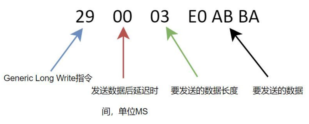
From the analysis, it can be seen that the data E0 AB BA is the initialization sequence sent to the MIPI, corresponding to the code SSD_SEND(0x01,0xE0,0xAB,0xBA) provided by the screen supplier.
0x29 is the Generic Long Write command. There are also Generic Write commands:
| Data Type (hex) | Data Type (binary) | Description | Packet Size |
|---|---|---|---|
| 0x03 | 00 0011 | Generic Short WRITE, no parameters | Short |
| 0x13 | 01 0011 | Generic Short WRITE, 1 parameter | Short |
| 0x23 | 10 0011 | Generic Short WRITE, 2 parameters | Short |
| 0x29 | 10 1001 | Generic Long Write | Long |
If n < 3, the Payload will be packed in the form of a Short Packet. n is the number of parameters. Among them:
- n = 0 means there are no parameters, and the command is 0x03.
- n = 1 means 1 parameter, and the command is 0x13.
- n = 2 means 2 parameters, and the command is 0x23.
- When n >= 3, the payload will be packed in the form of a Long Packet, representing n parameters, and command 0x29 is selected.
In addition to the Generic Write command, there is also the DCS Write command.
| Data Type (hex) | Data Type (binary) | Description | Packet Size |
|---|---|---|---|
| 0x05 | 00 0101 | DCS Short WRITE, no parameters | Short |
| 0x15 | 01 0101 | DCS Short WRITE, 1 parameter | Short |
| 0x39 | 11 1001 | DCS Long Write/write_LUT Command Packet | Long |
If n < 2, n is the number of parameters. The data to be sent will be packed in the form of a Short Packet.
- n = 0 means no parameters, and command 0x05 is selected.
- n = 1 means one parameter, and command 0x15 is selected.
- When n >= 2, the data to be sent will be packed in the form of a Long Packet. At this point, the DCS command is sent with n parameters, and command 0x39 is selected.
panel-init-sequenceandpanel-exit-sequenceThe analysis methods for other initialization sequences corresponding to the attributes are the same as in this example, and you can analyze them on your own.
Set backlight and touch
arch/arm64/boot/dts/rockchip/topeet-screen-lcds.dtsAdd the following code:
12345678910111213 | &pwm5{ status = "okay";};&backlight1{ pwms = <&pwm5 0 25000 0>; status = "okay";};&ft5x061{ status = "okay";}; |
Set screen logo
arch/arm64/boot/dts/rockchip/topeet-screen-lcds.dtsAdd the following code:
1234 | &route_dsi1{ status = "okay"; connect = <&vp1_out_dsi1>;}; |
HDMI screen porting
HDMI interface introduction
Background
In 1998, computer industry giants such as Intel, IBM, HP, Fujitsu, and Compaq jointly launched the DVI (Digital Visual Interface) interface. The DVI interface is based on TMDS (Transition Minimized Differential Signaling) technology to transmit digital signals. Through an encoding algorithm, 8-bit data (each primary color signal in R, G, B) is encoded into 10-bit data (including horizontal and vertical sync information, clock information, data DE, error correction, etc.), and differential signaling is used to transmit data.
The DVI interface is widely used in devices such as PCs, DVDs, high-definition televisions (HDTV), and high-definition projectors. It can support resolutions up to 2K@60Hz and 1080P@120Hz. However, with the popularity of high-definition television (HDTV) in the early 21st century, consumer demand for audio-video integration surged. TV manufacturers (such as Sony, Panasonic, Hitachi, etc.) believed that DVI could not meet the following requirements:
- TV and home theater equipment are becoming thinner and lighter, requiring more compact interfaces to achieve device miniaturization. However, the DVI interface is bulky and inconvenient to plug and unplug, making it difficult to adapt to thin and light devices.
- Digital audio and video need to be transmitted through a single interface to achieve audio-video integration, but the DVI interface has a single function, only supporting video transmission, requiring additional cables for audio transmission.
- The problem of piracy of high-definition content is serious, and the demand for encryption technology is increasing. However, the DVI interface does not integrate content encryption technology (such as HDCP).
- It is necessary to support higher bandwidth to support emerging resolutions such as 4K and 8K. The DVI interface has limited bandwidth and is difficult to meet the growing resolution requirements.
In 2002, TV manufacturers such as Sony, Panasonic, Hitachi, Toshiba, and Philips jointly established the HDMI Alliance, with the goal of designing a next-generation interface to replace DVI, namely the HDMI interface. The full name of the HDMI interface is High Definition Multimedia Interface, which is the high-definition multimedia interface. In 2003, the HDMI 1.0 standard was officially released, and its core features include:
- High bandwidth: 5Gbps transmission rate, supporting 1080P@60Hz and uncompressed 8-channel audio.
- Interface miniaturization: about 50% smaller than DVI, making plugging and unplugging more convenient.
- Audio-video integration: transmits digital video and audio signals over a single cable.
- Compatibility: backward compatible with the DVI interface through an adapter.
- Content protection: Integrated HDCP encryption technology to prevent illegal copying.
The development history of HDMI
HDMI 1.2 (2005): Supports display color depth expansion (8/10/12bit), compatible with SACD audio.
HDMI 1.3 (2006): Bandwidth increased to 10.2Gbps, introducing Deep Color technology and xvYCC wide color gamut.
HDMI 1.4 (2009): Bandwidth 10.2Gbps, new features: support for 4K@30Hz, 1080P@144Hz, 3D video. Added Ethernet channel (HEC) and Audio Return Channel (ARC).
HDMI 2.0a/b (2013-2016): Bandwidth 18Gbps, supports 4K@60Hz, 1080P@240Hz, introduces static HDR (High Dynamic Range).
HDMI 2.1 (2017): Bandwidth leaps to 48Gbps, core upgrades: resolution and refresh rate: 8K@60Hz, 4K@120Hz (uncompressed), supports dynamic HDR (Dolby Vision); gaming optimization: Variable Refresh Rate (VRR), Auto Low Latency Mode (ALLM); enhanced audio: eARC (enhanced Audio Return Channel).
HDMI connector pin definitions
There are five HDMI connector types, A to E.
- The HDMI-A connector, also called the standard connector, is the most widely used.

Pin definitions:
| Pin number | Function | Pin number | Function |
|---|---|---|---|
| 1 | TMDS Data 2+ | 10 | TMDS Clock + |
| 2 | TMDS Data Shield | 11 | TMDS Clock Shield |
| 3 | TMDS Data 2- | 12 | TMDS Clock - |
| 4 | TMDS Data 1+ | 13 | CEC |
| 5 | TMDS Data 1 Shield | 14 | Reserved |
| 6 | TMDS Data 1- | 15 | SCL(DDC CLOCK) |
| 7 | TMDS Data 0+ | 16 | SDA(DDC DATA) |
| 8 | TMDS Data 0 Shield | 17 | GND |
| 9 | TMDS Data 0- | 18 | +5V Power |
| 19 | HPD Hot Plug Detect |
- The HDMI-B interface is basically not seen in daily use. The data transmission capability of the HDMI-B interface is nearly 2 times faster than HDMI-A, and it is generally used in more professional scenarios.

- HDMI-C is also called Mini HDMI, a mini HDMI interface. Its size is nearly one-third smaller than HDMI-A, and it is mainly used in small devices, such as game consoles, digital cameras, etc.

Pin definitions:
| Pin number | Function | Pin number | Function |
|---|---|---|---|
| 1 | TMDS Data 2 Shield | 10 | TMDS Clock Shield |
| 2 | TMDS Data 2+ | 11 | TMDS Clock + |
| 3 | TMDS Data 2- | 12 | TMDS Clock - |
| 4 | TMDS Data 1 Shield | 13 | CEC/DDC Ground |
| 5 | TMDS Data 1+ | 14 | CEC |
| 6 | TMDS Data 1- | 15 | SCL(DDC CLOCK) |
| 7 | TMDS Data 0 Shield | 16 | SDA(DDC DATA) |
| 8 | TMDS Data 0+ | 17 | HEC+ |
| 9 | TMDS Data 0- | 18 | +5V Power |
| 19 | HPD Hot Plug Detect / HEC− |
- The HDMI-D interface is also called Micro HDMI, a micro HDMI interface. Micro HDMI is also relatively small, mainly used in small mobile devices, such as tablets, portable car devices, etc.

Pin definitions:
- The HDMI-E interface is mainly used in automotive systems. Due to the unstable environment inside the vehicle, the HDMI-E interface adopts a mechanical locking design on the physical connector to ensure contact reliability.
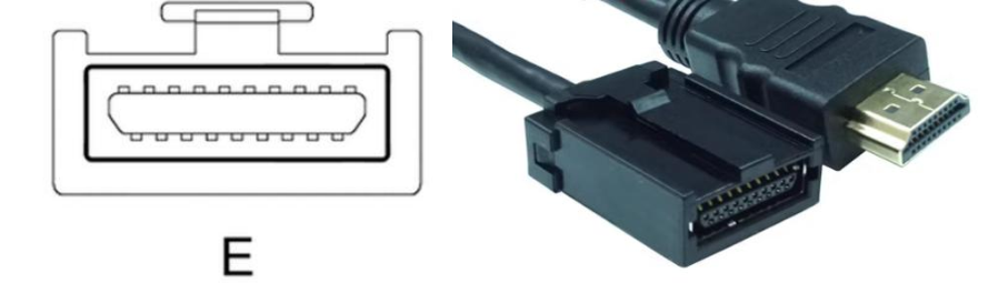
| Pin number | Function | Pin number | Function |
|---|---|---|---|
| 1 | HPD Hot Plug Detect / HEC− | 10 | TMDS Data 0 Shield |
| 2 | Utility/HEAC+ | 11 | TMDS Data 0− |
| 3 | TMDS Data 2+ | 12 | TMDS Clock + |
| 4 | TMDS Data 2 Shield | 13 | TMDS Clock Shield |
| 5 | TMDS Data 2− | 14 | TMDS Clock− |
| 6 | TMDS Data 1+ | 15 | CEC |
| 7 | TMDS Data 1 Shield | 16 | DDC/CEC/HEAC |
| 8 | TMDS Data 1− | 17 | SCL (DDC CLOCK) |
| 9 | TMDS Data 0+ | 18 | SDA (DDC DATA) |
| 19 | +5V Power |
RK3568 HDMI Interface
The RK3568 processor supports one HDMI interface, which can support both 1.4a and 2.0a versions. It supports up to 4K@60Hz resolution.

Bandwidth Calculation
When selecting an HDMI screen, how do you determine whether the processor can support a screen with that resolution? This involves HDMI bandwidth calculation. Take the RK3568 processor as an example.
The RK3568 processor supports up to HDMI 2.0. In HDMI 2.0, the TMDS clock is 600 MHz, so the bandwidth under HDMI 2.0 is: 600000000 x 10 x 3 = 18 Gbps.
The effective bandwidth is 18 x (8/10) = 14.4 Gbps.
Why should the effective bandwidth be multiplied by 8/10? Because HDMI transmission uses 8b/10b encoding, which converts 8-bit data into 10 bits for transmission. Therefore, the effective data bandwidth is only 8/10 of the raw bandwidth. Then we calculate the bandwidth required by the HDMI display. If the bandwidth required by the HDMI display is less than the processor’s HDMI bandwidth, then the display can be supported.
HDMI display bandwidth calculation formula:Htotal x Vtotal x refresh rate x encoding format x bit depth
Here, Htotal equals Hsync + Hfront + Hactive + Hback, and Vtotal equals Vsync + Vfront + Vactive + Vback. Htotal x Vtotal represents the number of pixels per frame.
The number of pixels per frame multiplied by the display refresh rate gives the number of pixels the display needs to process per second, i.e., Htotal x Vtotal x refresh rate. If the encoding format is yuv444, the encoding value is 1; if the encoding format is yuv422, the encoding value is 2/3; if the encoding format is yuv420, the encoding value is 1/2.
For example: a display with 3920 (Htotal) x 2222 (Vtotal) @60Hz, using yuv444 encoding and 8-bit depth, requires a bandwidth of 3920x2222x60x1x8x3, which is approximately 12.543 Gbps.
If you don’t want to calculate, you can also determine it by looking up a table. From the table below, for example, HDMI 2.0 supports a maximum resolution of 4K@120Hz.

Introduction to TMDS Differential Signals
Earlier we mentioned that the DVI interface uses TMDS differential signals, and the HDMI interface was developed to replace the DVI interface.
In fact, HDMI originates from DVI interface technology. The HDMI interface is also centered on the TMDS signal transmission technology of Silicon Image, Inc. HDMI is pin-compatible with DVI, but uses a different package. Therefore, HDMI and DVI interfaces can be converted to each other through adapter connectors. In principle, HDMI is backward compatible with DVI.
Therefore, this section focuses on introducing TMDS differential signals. We start with the connection framework diagram in the HDMI specification.

As can be seen from the figure, TMDS transmission is divided into two parts: the source (transmitter) and the sink (receiver). The TMDS link includes 3 data transmission channels (Channel 0, 1, 2) and 1 clock signal transmission channel (Clock Channel).
Taking the source on the left as an example, there are 3 data channels in total. Each data channel uses parallel transmission with a width of 8 bits. Among them:
- D[7:0]: represents 8 bits of actual image data.
- D[1:0]: In Channel 0, it represents the HSYNC and VSYNC signals; in Channel 1 and Channel 2, it represents the four control signals CTL0~CTL3.
- D[3:0]: used to represent some additional auxiliary data, such as audio data, etc.
Why does this 8-bit data D[7:0] already transmit image data, and how can D[1:0] also transmit other signals?

In the HDMI transmission overview diagram, transmission is divided into 3 phases. These three transmission phases are: dark gray for the video data period, dark blue for the data island period, and light gray for the control period.

- Control Period
When there is no need to transmit video, audio, or auxiliary data, the control period is used. There must be a control period between any two non-control periods. It uses CTL encoding to convert 2-bit data into 10-bit data.
Before each Video Data Period or Data Island Period, a preamble is sent via the Control Period. The preamble is a sequence of eight identical control characters, used to indicate whether the following data period is a Video Data Period or a Data Island Period.

The values of CTL0, CTL1, CTL2, and CTL3 indicate the type of the subsequent data period, and the remaining control signals (HSYNC and VSYNC) may also change.

- Data Island Period
In this phase, audio and other auxiliary data are transmitted, using TERC4 encoding, which converts 4-bit data into 10-bit data. The Data Island Period consists of three parts: leading guard band, data header and data packet, and trailing guard band.

- Video Data Period
In this phase, actual image data is transmitted, using video data encoding, which converts 8-bit data into 10-bit data. The Video Data Period has a leading guard band but no trailing guard band.

It can be seen that D[7:0] does not transmit these data simultaneously, but transmits them in stages.
TMDS is a differential signal, and LVDS is also a differential signal. What is the difference between them?
For the working principle of LVDS differential signals, see the LVDS Interface Introduction chapter.
TMDS differential signals use 2 differential lines to transmit signals. Signal 0 and 1 are determined by the voltage difference between the two pins:
- When the TMDS differential line + is high,
- and the differential line - is low, it represents 1;
- When the differential line + is low and the differential line - is high, it represents 0.
- The TMDS receiver determines whether the transmitted data is 1 or 0 by judging the voltage difference between + and -.
EDID Introduction
Different types and brands of monitors have different resolutions and timings. The HDMI interface must be compatible. If the processor outputs a fixed resolution and timing parameters, it cannot drive all monitors well.
EDID stands for Extended Display Identification Data, which is external display device identification data. EDID contains monitor-related parameters such as resolution and timing information, as well as manufacturer information, product ID, production date, and so on. For example, address 08h in the EDID structure diagram below occupies 2 bytes and is used to represent the manufacturer name, using the ISA 3-character ID code. The same applies to other addresses; you can read the EDID structure diagram yourself.
The EDID length for HDMI is generally 256 bytes, divided into 2 blocks: Block 0 (corresponding to 00h-36h in the EDID structure diagram below) and Block 1 (corresponding to 36h-7fh in the EDID structure diagram below). Block 0 is mandatory, while Block 1 is optional.
EDID v1.4 version structure:
| Address | Bytes | Description | Format |
|---|---|---|---|
| 00h | 8 | Header: = (00 FF FF FF FF FF FF 00h) | See Section 3.3 |
| 08h | 10 | Vendor & Product Identification: | See Section 3.4 |
| 08h | 2 | ID Manufacturer Name | ISA 3-character ID Code |
| 0Ah | 2 | ID Product Code | Vendor assigned code |
| 0Ch | 4 | ID Serial Number | 32-bit serial number |
| 10h | 1 | Week of Manufacture | Week number or Model Year Flag |
| 11h | 1 | Year of Manufacture or Model Year | Manufacture Year or Model Year |
| 12h | 2 | EDID Structure Version & Revision: | See Section 3.5 |
| 12h | 1 | Version Number: = 01h | Binary |
| 13h | 1 | Revision Number: = 04h | Binary |
| 14h | 5 | Basic Display Parameters & Features: | See Section 3.6 |
| 14h | 1 | Video Input Definition | See Section 3.6.1 |
| 15h | 1 | Horizontal Screen Size or Aspect Ratio | Listed in cm. → Aspect Ratio — Landscape |
| 16h | 1 | Vertical Screen Size or Aspect Ratio | Listed in cm. → Aspect Ratio — Portrait |
| 17h | 1 | Display Transfer Characteristic (Gamma) | Binary — Factory Default Value |
| 18h | 1 | Feature Support | See Section 3.6.4 |
| 19h | 10 | Color Characteristics: | See Section 3.7 |
| 19h | 1 | Red/Green: Low Order Bits | Rx0 Rx1 Ry0 Ry1 Gx0 Gx1 Gy0 Gy1 |
| 1Ah | 1 | Blue/White: Low Order Bits | Bx0 Bx1 By0 By1 Wx0 Wx1 Wy0 Wy1 |
| 1Bh | 1 | Red-x: High Order Bits | Red-x Bits 9 → 2 |
| 1Ch | 1 | Red-y: High Order Bits | Red-y Bits 9 → 2 |
| 1Dh | 1 | Green-x: High Order Bits | Green-x Bits 9 → 2 |
| 1Eh | 1 | Green-y: High Order Bits | Green-y Bits 9 → 2 |
| 1Fh | 1 | Blue-x: High Order Bits | Blue-x Bits 9 → 2 |
| 20h | 1 | Blue-y: High Order Bits | Blue-y Bits 9 → 2 |
| 21h | 1 | White-x: High Order Bits | White-x Bits 9 → 2 |
| 22h | 1 | White-y: High Order Bits | White-y Bits 9 → 2 |
| 23h | 3 | Established Timings | See Section 3.8 |
| 23h | 1 | Established Timings I | |
| 24h | 1 | Established Timings II | |
| 25h | 1 | Manufacturer’s Reserved Timings | |
| 26h | 16 | Standard Timings: Identification 1 → 8 | See Section 3.9 |
| 36h | 72 | 18 Byte Data Blocks | See Section 3.10 |
| 36h | 18 | Preferred Timing Mode | |
| 48h | 18 | Detailed Timing #2 or Display Descriptor | |
| 5Ah | 18 | Detailed Timing #3 or Display Descriptor | |
| 6Ch | 18 | Detailed Timing #4 or Display Descriptor | |
| 7Eh | 1 | Extension Block Count N | Number of (optional) 128-byte EDID EXTENSION blocks to follow – if Block Maps are used then 00h ≤ N ≤ FEh and FFh is invalid.Maps are used then 254 is the maximum value of ‘N’. If Block Maps are not used then 255 is the maximum value of ‘N’. 00h ≤ N ≤ FFh. |
| 7Fh | 1 | Checksum C | 00h ≤ C ≤ FFhThe 1-byte sum of all 128 bytes in this EDID block shall equal zero |
In this way, by reading the EDID information, appropriate display parameters can be output to be compatible with HDMI screens from different manufacturers and brands. In some materials, you may also see E-EDID, which stands for Enhanced Extended Display Identification Data. E-EDID and EDID are just different versions in the development of this technology. E-EDID is backward compatible with EDID, so they can be treated as the same.
Currently, the DRM driver already supports the vast majority of resolution timings, but in some special scenarios, there may be some special resolutions that are not supported. You candrivers\gpu\drm\drm_edid.cindrm_dmt_modesAdd screen information at the end.
123 | { DRM_MODE("4096x2160", DRM_MODE_TYPE_DRIVER, 556188, 4096, 4104,4136, 4176, 0, 2160, 2208, 2216, 2222, 0,DRM_MODE_FLAG_PHSYNC | DRM_MODE_FLAG_NVSYNC) }, |
| Parameters | Description |
|---|---|
| “4096x2160” | mode name, which is hdisplay × vdisplay of the resolution |
| DRM_MODE_TYPE_DRIVER | mode type, configured as DRM_MODE_TYPE_DRIVER |
| 556188 | Pixel clock (unit: kHz) |
| 4096 | Horizontal active pixels (hdisplay) |
| 4104 | Horizontal sync start pixel (hsync_start) |
| 4136 | Horizontal sync end pixel (hsync_end) |
| 4176 | Total pixels per line (htotal) |
| 0 | hskew, usually 0 |
| 2160 | Vertical active lines (vdisplay) |
| 2208 | Vertical sync start line (vsync_start) |
| 2216 | Vertical sync end line (vsync_end) |
| 2222 | Total lines per frame (vtotal) |
| 0 | vscan, usually 0 |
| vrefresh | Display device frame rate |
| DRM_MODE_FLAG_PHSYNC | hsync and vsync polarity, flags are defined as follows: DRM_MODE_FLAG_PHSYNC (1<<0)DRM_MODE_FLAG_NHSYNC (1<<1)DRM_MODE_FLAG_PVSYNC (1<<2)DRM_MODE_FLAG_NVSYNC (1<<3)DRM_MODE_FLAG_INTERLACE (1<<4) |
Hardware schematic analysis
The iTOP-RK3568 development board has an HDMI interface, and the interface schematic is as follows:

- HDMI_TX2P_PORT/HDMI_TX2N_PORT、HDMI_TX1P_PORT/HDMI_TX1N_PORT、HDMI_TX0P_PORT/HDMI_TX0N_PORT、HDMI_TXCLKP_PORT/HDMI_TXCLKN_PORT consists of 3 pairs of data pins and 1 pair of clock pins.
- HDMI_TX_CEC_PORT, CEC pin.
- HDMI_TXDDC_SCL_PORT/HDMI_TXDDC_SDA_PORT. DDC channel pins, communicate via I2C, mainly used to read EDID information.
- HDMI_TX_HPD_PORT hot-plug detection pin.
Adaptation steps
rk3568.dtsiThe hdmi node is as follows:
123456789101112131415161718192021222324252627282930313233343536373839404142 | hdmi: hdmi@fe0a0000 { compatible = "rockchip,rk3568-dw-hdmi"; reg = <0x0 0xfe0a0000 0x0 0x20000>; interrupts = <GIC_SPI 45 IRQ_TYPE_LEVEL_HIGH>; clocks = <&cru PCLK_HDMI_HOST>, <&cru CLK_HDMI_SFR>, <&cru CLK_HDMI_CEC>, <&pmucru PLL_HPLL>, <&cru HCLK_VOP>; clock-names = "iahb", "isfr", "cec", "ref", "hclk"; power-domains = <&power RK3568_PD_VO>; reg-io-width = <4>; rockchip,grf = <&grf>; pinctrl-names = "default"; pinctrl-0 = <&hdmitx_scl &hdmitx_sda &hdmitxm0_cec>; status = "disabled"; ports { port@0 { reg = <0>; hdmi_in_vp0: endpoint@0 { reg = <0>; remote-endpoint = <&vp0_out_hdmi>; status = "disabled"; }; hdmi_in_vp1: endpoint@1 { reg = <1>; remote-endpoint = <&vp1_out_hdmi>; status = "disabled"; }; }; };}; |
compatibleattribute value isrockchip,rk3568-dw-hdmi, indicating that it will be usedgpu/drm/rockchip/dw_hdmi-rockchip.c this driver.
pinctrl-0 = <&hdmitx_scl &hdmitx_sda &hdmitxm0_cec>;: Use pinctrl to set the multiplexing of the scl, sda, and cec pins.
statusThe property value is disabled, indicating that this node is disabled. Because HDMI is to be used, the node needs to be enabled later.
portsThe node represents the VP port corresponding to the HDMI interface. hdmi_in_vp0 indicates that the HDMI interface is connected to VP0. hdmi_in_vp1 indicates that the HDMI interface is connected to VP1.statusThe property value disabled means that outputting HDMI via VP0/1 is prohibited.
arch/arm64/boot/dts/rockchip/topeet-screen-lcds.dtsas follows
123456789101112131415161718192021222324252627282930313233343536373839404142434445464748495051 | &hdmi { status = "okay"; rockchip,phy-table = <92812500 0x8009 0x0000 0x0270>, <165000000 0x800b 0x0000 0x026d>, <185625000 0x800b 0x0000 0x01ed>, <297000000 0x800b 0x0000 0x01ad>, <594000000 0x8029 0x0000 0x0088>, <000000000 0x0000 0x0000 0x0000>;};&hdmi_in_vp0 { status = "okay";};&hdmi_in_vp1 { status = "disabled";};&hdmi_sound { status = "okay";};&route_hdmi { status = "okay"; connect = <&vp0_out_hdmi>;};&hdmi { status = "okay"; rockchip,phy-table = <92812500 0x8009 0x0000 0x0270>, <165000000 0x800b 0x0000 0x026d>, <185625000 0x800b 0x0000 0x01ed>, <297000000 0x800b 0x0000 0x01ad>, <594000000 0x8029 0x0000 0x0088>, <000000000 0x0000 0x0000 0x0000>;};&hdmi_in_vp0 { status = "disabled";};&hdmi_in_vp1 { status = "okay";};&hdmi_sound { status = "okay";};&route_hdmi { status = "okay"; connect = <&vp1_out_hdmi>;}; |
eDP Screen Porting
eDP Interface Introduction
eDP stands for Embedded DisplayPort, an embedded display interface founded by the Video Electronics Standards Association (VESA). The eDP protocol is an extension of the DP (DisplayPort) architecture and protocol for embedded applications, so the eDP protocol is fully compatible with the DP protocol. It has been widely used in laptops, tablets, and other fields.
RK3568 supports 1 eDP interface. Features are as follows:
- Supports 1 eDP 1.3 interface
- Up to 4 physical lanes, each lane supports 2.7 Gbps
- Supports Panel Self Refresh (PSR)
- Supports a maximum resolution of 2560x1600 @ 60Hz
- Supports RGB format (up to 10-bit color depth)
The iTOP-RK3568 development board brings out 1 eDP interface. The schematic is as follows:

- EDP_TX_D0N/EDP_TX_D0P、EDP_TX_D1N/EDP_TX_D1P、EDP_TX_D2N/EDP_TX_D2P、EDP_TX_D3N/EDP_TX_D3P. It consists of 4 differential pairs, used to transmit audio and video data. Note that the specific LCD screen uses as many differential pairs as it requires: if 2 pairs are needed, connect 2 pairs; if 4 pairs are needed, connect 4 pairs.
- EDPAUXN/EDPAUXP auxiliary channel.
- EDP_HPDIN_M1 hot-plug pin, not used in the schematic. That is, this pin is optional.
- I2C1_SCL_TP、I2C1_SDA_TP、TP_INT_L_GPIO3_A5、TP_RST_L_GPIO0_B6, touch I2C communication, interrupt, and reset pins.
- LCD0_BL_PWM4 screen backlight pin.
Adaptation steps
rk3568.dtsiThe edp node is as follows:
1234567891011121314151617181920212223242526272829303132333435363738 | edp: edp@fe0c0000 { compatible = "rockchip,rk3568-edp"; reg = <0x0 0xfe0c0000 0x0 0x10000>; interrupts = <GIC_SPI 18 IRQ_TYPE_LEVEL_HIGH>; clocks = <&pmucru XIN_OSC0_EDPPHY_G>, <&cru PCLK_EDP_CTRL>, <&cru CLK_EDP_200M>, <&cru HCLK_VO>; clock-names = "dp", "pclk", "spdif", "hclk"; resets = <&cru SRST_EDP_24M>, <&cru SRST_P_EDP_CTRL>; reset-names = "dp", "apb"; phys = <&edp_phy>; phy-names = "dp"; power-domains = <&power RK3568_PD_VO>; status = "disabled"; ports { edp_in: port@0 { reg = <0>; edp_in_vp0: endpoint@0 { reg = <0>; remote-endpoint = <&vp0_out_edp>; status = "disabled"; }; edp_in_vp1: endpoint@1 { reg = <1>; remote-endpoint = <&vp1_out_edp>; status = "disabled"; }; }; };}; |
compatibleattribute value isrockchip,rk3568-edp, indicating that it will be usedgpu/drm/rockchip/analogix_dp-rockchip.cthis driver.
phys = <&edp_phy>;It uses edp_phy, so we need to enable the edp_phy node.
statusThe attribute value is disabled, indicating that the eDP node is disabled, so we need to enable the eDP node.
portsThe node represents the VP port corresponding to the eDP interface. edp_in_vp0 indicates that the eDP interface is connected to VP0,edp_in_vp1indicates that the eDP interface is connected to VP1, and the status attribute value disabled means that eDP output is disabled.
arch/arm64/boot/dts/rockchip/topeet-screen-lcds.dtsas follows
1234567891011121314151617181920212223 | &edp { hpd-gpios = <&gpio0 RK_PC0 GPIO_ACTIVE_HIGH>; status = "okay";};&edp_phy { status = "okay";};&edp_in_vp0 { status = "okay";};&edp_in_vp1 { status = "disabled";};&route_edp { status = "okay"; connect = <&vp0_out_edp>;}; |
VGA screen porting
VGA interface introduction
VGA stands for Video Graphics Array, which is a video graphics array. VGA is a protocol that uses analog signals for video transmission, introduced by IBM in 1987. Initially, due to its high resolution, fast display speed, and rich colors, it was very common in desktop computer applications. However, the VGA interface is relatively large, and as portable laptops become increasingly popular, it has been gradually phased out in the pursuit of thin and light laptops.
VGA interfaces are divided into male and female connectors. When transmitting images between the two, the VGA image transmission standard is used.

| Pin Number | Name | Direction | Function description |
|---|---|---|---|
| 1 | RED | → | Red video signal |
| 2 | GREEN | → | Green video signal |
| 3 | BLUE | → | Blue video signal |
| 4 | RES | – | Reserved |
| 5 | GND | → | Ground |
| 6 | RGND | → | Red ground |
| 7 | GGND | → | Green ground line |
| 8 | BGND | → | Blue ground line |
| 9 | +5V | → | +5V DC power supply |
| 10 | SGND | → | Sync ground line |
| 11 | ID0 | → | Monitor ID bit 0 (optional) |
| 12 | SDA | → | DDC serial data line |
| 13 | HSYNC or CSYNC | → | Horizontal sync signal (or composite sync signal) |
| 14 | VSYNC | → | Vertical sync signal |
| 15 | SCL | → | DDC data clock line |
The RK3568 processor itself does not have a VGA interface; the VGA interface on the iTOP-RK3568 development board is converted from the eDP interface.
Hardware schematic analysis

The eDP-to-VGA interface schematic is very simple, using an RTD2166 conversion chip. The input of the conversion chip is the eDP signal. After passing through the conversion chip, it outputs a VGA signal.
Among them, EDP_TX_D0P/EDP_TX_D0N、EDP_TX_D1P/EDP_TX_D1N、EDP_TX_AUXP/EDP_TX_AUXN. Two pairs of differential lines are used to transmit audio/video data. EDPAUXN/EDPAUXP are auxiliary channels. VGA_HPDIN_GPIO0_C0 is the hot-plug pin. I2C5_SDA_M0/I2C5_SCL_M0 is the conversion chip control pin.
VGA_R、VGA_G、VGA_B、VGA_HSYNC、VGA_VSYNC、VGA_DDC_SDA、VGA_DDC_SCL is the output pin of the conversion chip, which is the converted VGA signal; just connect it to the VGA connector.
Adaptation steps
1234567891011121314151617181920212223 | &edp { hpd-gpios = <&gpio0 RK_PC0 GPIO_ACTIVE_HIGH>; status = "okay";};&edp_phy { status = "okay";};&edp_in_vp0 { status = "okay";};&edp_in_vp1 { status = "disabled";};&route_edp { status = "okay"; connect = <&vp0_out_edp>;}; |