
Timeline
Timeline
2026-01-14
init
This article introduces the basics of ADC (Analog-to-Digital Converter) in Linux driver notes. It first distinguishes the characteristics and application scenarios of analog and digital signals, then elaborates on the four steps of ADC converting analog signals to digital signals: sampling, holding, quantization, and encoding, and explains the definition, function, and key parameters of each step. The article also lists typical applications of ADC in sensor signal acquisition, audio processing, image processing, industrial automation, and medical equipment, and briefly mentions the concept of ADC resolution and its impact on signal accuracy.
Linux Driver Notes
| Table of Contents | Links |
|---|---|
| 1. Linux Driver Framework | |
| 2. Linux Driver Loading Logic | |
| 3. Character Device Basics | |
| 4. Concurrency and Race Conditions | |
| 5. Advanced Character Device Topics | |
| 6. Interrupts | |
| 7. Platform Bus | |
| 8. Device Tree | |
| 9. Device Model | |
| 10. Hotplug | |
| 11. pinctrl Subsystem | |
| 12. GPIO subsystem | |
| 13. Input subsystem | |
| 14. 1-Wire | |
| 15. I2C | |
| 16. SPI | |
| 17. UART | |
| 18. PWM | |
| 19. RTC | |
| 20. Watchdog | |
| 21. CAN | |
| 22. Network devices | |
| 23. ADC | |
| 24. IIO | |
| 25. USB | |
| 26. LCD |

ADC Basics
Analog and Digital Signals
Analog SignalIt is a continuously varying signal whose value can take any value within a certain range. It is continuous in both time and amplitude, and can accurately reflect changes in physical quantities in nature. For example, voltage signals output by temperature sensors, sound signals picked up by microphones, and light intensity signals detected by photoresistors all fall into the category of analog signals.
Digital SignalIt is a discrete signal whose value can only take specific values within a limited range, usually expressed in binary form. It is characterized by being discrete in time (with fixed time intervals between sampling points) and discrete in amplitude (quantized values). For example, data stored and processed in computers, audio data in MP3 files, and pixel values in JPEG image files are all concrete manifestations of digital signals.
| Dimension | Analog signal characteristics | Digital signal characteristics |
|---|---|---|
| Essence | Continuous variation, arbitrary values | Discrete values, often represented in binary |
| Features | Both time and amplitude are continuous | Both time (sampling interval) and amplitude (quantized value) are discrete |
| Advantages | Accurately reflects changes in natural physical quantities | Easy to store/transmit/process, strong anti-interference capability |
| Typical scenarios | Raw sensor signals, natural acoustic, optical, and electrical signals | Computer data, digital audio and video files |
ADC Concept
ADC is Analog-to-Digital Converter the abbreviation for, which can be translated asAnalog-to-Digital Converter. It is an electronic device or circuit module used forConvert continuously varying analog signals (such as voltage, current, etc.) into discrete digital signals. These digital signals can be processed and stored by computers, microcontrollers, or other digital systems.
. The conversion of analog signals to digital signals by an ADC is usually divided intoSampling、Holding、QuantizationandEncodingfour steps. The definition and function of each step are shown in the following table:
| Step | Definition | Function | Key parameters or characteristics |
|---|---|---|---|
| Sampling | The process of measuring an analog signal at fixed time intervals. | Discretizes the time-continuous analog signal, laying the foundation for subsequent digital processing. | Sampling Rate, i.e., the number of samples per second. According to the Nyquist sampling theorem, the sampling rate must be at least twice the highest frequency of the signal. |
| Holding | After sampling, the instantaneous value of the signal is held for a period of time for subsequent processing. | Ensures that the signal does not distort due to rapid changes during quantization, improving the accuracy and stability of the conversion. | No specific parameter; the main purpose is to stabilize the signal. |
| Quantization | The process of mapping the continuous amplitude obtained by sampling to a set of discrete values. | Discretizes the amplitude-continuous signal so that it can be represented by digital systems. | Resolution, usually expressed in bits (e.g., 8-bit, 10-bit, 12-bit, etc.). The higher the resolution, the more accurate the signal. |
| Encoding | The process of converting the quantized values into binary code. | Represents the discrete values in a form recognizable by digital systems, facilitating storage, transmission, and processing, so that analog signals can be used by computers or other digital devices. | No specific parameter; the focus is on generating binary code suitable for use by digital systems. |
ADCs are widely used in sensor signal acquisition, audio processing, image processing, industrial automation, and medical devices:
- Sensor signal acquisition: Many sensors output analog signals. For example, environmental data collected by temperature sensors, pressure sensors, photosensitive sensors, etc., usually exists in the form of analog signals.
- Audio processing: The sound signal picked up by a microphone is an analog signal.
- Image processing: The light signal captured by a camera is essentially an analog signal.
- Industrial automation: The measurement of various physical quantities (such as speed, position, pressure, etc.) usually relies on analog signals output by sensors.
- Medical devices: Many biological signals (such as ECG, EEG, etc.) are acquired in the form of analog signals.
ADC Resolution
The resolution of an ADC refers to the ability of the analog-to-digital converter to distinguish the smallest signal change. In other words, it is the fineness with which the ADC quantizes an analog signal into discrete digital values. In an ADC, the higher the resolution, the more accurately it can represent the input analog signal. When we restore a digital signal to an analog signal through a DAC (digital-to-analog converter), a high-resolution ADC can generate a result closer to the original analog signal.
The resolution of an ADC is usually expressed in bits, such as 8-bit, 10-bit, 12-bit, etc. The number of bits determines the number of discrete values the ADC can output. An n-bit ADC can represent 2^n different values. For example, an 8-bit ADC can represent 2^8=256 different values; a 10-bit ADC can represent 2^10=1024 different values; a 12-bit ADC can represent 2^12=4096 different values. The higher the number of bits, the higher the resolution, and the smaller the signal change that can be distinguished.
Resolution can be calculated using the following formula:
Where:
- Range refers to the maximum range of the ADC input signal (i.e., the reference voltage range);
- n is the number of bits of the ADC;
- 2^n represents the total number of discrete values the ADC can distinguish.
Example: Suppose a 3-bit ADC has a reference voltage (range) of 2V, calculate its resolution:
- Range = 2V
- The number of bits is 3, 2^n = 2^3 = 8;
Substituting into the resolution calculation formula gives 2V/8 = 0.25V. This means the ADC can divide the input signal into 8 discrete levels, with a step size of 0.25V between each level.
In addition to resolution, other parameters of the ADC are as follows
| Parameters | Definition | Function or Significance |
|---|---|---|
| Sampling Time | The time required to complete one sampling. | Determines how quickly the ADC can capture changes in the input signal. If the sampling time is too long, it may cause signal distortion or loss of detail. |
| Conversion Time | The time required to convert an analog signal to a digital signal. | Directly affects the speed and efficiency of the ADC. A shorter conversion time means the ADC can process signals faster. |
| Sampling Frequency | The number of samples collected per second, commonly expressed in ksps (thousands of samples per second) or Msps (millions of samples per second). | It determines the ADC’s ability to capture signal changes. According to the Nyquist sampling theorem, the sampling frequency must be at least twice the highest frequency of the signal to accurately reconstruct the signal. |
| Accuracy | The error between the digital value output by the ADC and the actual analog input value. | It reflects the reliability and measurement quality of the ADC and is an important indicator of its performance. |
RK3568 ADC
It can be found in the peripheral resource block diagram in the RK3568 datasheet. This RK3568 SoC has a total of 8-channel SARADC。
SARADC (Successive Approximation Register Analog-to-Digital Converterthe Chinese name of which isSuccessive Approximation ADC;
In addition to the SAR ADC, there are also two TS-ADC (Temperature Sensor ADC) channels, which are used to detect the temperature of the CPU and GPU respectively. If an excessively high temperature is detected within a period of time, an interrupt signal will be sent to the processor to take cooling measures; if the temperature continues to be too high, the entire chip will be reset to achieve a restart effect. The TS-ADC is only responsible for detecting the temperature of the CPU and GPU, so it is not brought out on the baseboard.
ADC Buttons
The ADC button is a SARADC peripheral. The working principle of the ADC button is:Multiple buttons are connected to the same ADC pin, and different voltages are generated through different voltage divider resistors. The ADC measures this voltage and compares it with a preset voltage range to determine which button is pressed.。
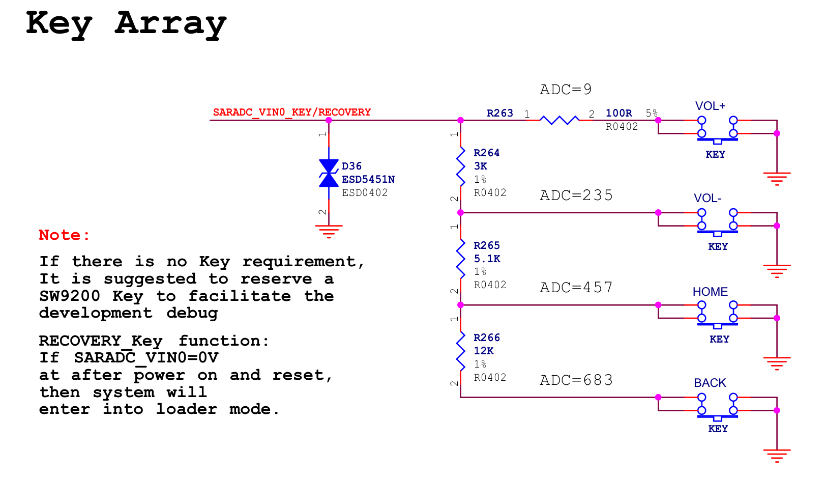
Two ADC channels are used for HW_ID and BOM_ID, used for hardware identification of different electronic devices. However, since topeet’s peripherals are universal, these two ADC channels are not used.


4 ADC channels are connected to a 6-pin connector, as shown in the schematic below.

The summary is as follows:
| ADC Interface | Multiplexed Function |
|---|---|
| SARADC VIN0 | Used as button pins (Volume +, Volume -, HOME, BACK) |
| SARADC VIN1 | Used as HW ID pin |
| SARADC VIN2 | Unused |
| SARADC VIN3 | Used as BOM ID pin |
| SARADC VIN4 | Unused |
| SARADC VIN5 | Unused |
| SARADC VIN6 | Unused |
| SARADC VIN7 | Unused |
Successive Approximation ADC
Successive approximation ADC (Successive Approximation Register ADCabbreviated as SAR ADC) is a common type of analog-to-digital converter, whose working principle is based on the successive approximation algorithm. It gradually compares the input analog signal with an internally generated reference voltage, and finally determines a digital value close to the input signal. The schematic diagram of the SAR ADC working principle is shown below.

As can be seen from the figure above, the successive approximation register analog-to-digital converter (SAR ADC) mainly consists of the following parts:
- Comparator: Used to compare the input analog signal U1 with the reference voltage U0 output by the D/A converter (DAC), and generate a feedback signal.
- N-bit D/A converter (DAC): Converts the digital value into an analog voltage, compares it with the input signal, and gradually approaches the target value.
- N-bit successive approximation register (SAR): Used to store the current comparison result, adjust the value according to the comparator’s feedback, and finally determine the digital output.
- Bit-setting selection logic: Controls the bit selection process of the successive approximation register, and adjusts the DAC output voltage using the binary search method.
Working process:
- First, the analog input signal U1 enters the ADC and is temporarily stored by the sampling circuit for subsequent processing.
- Then, the successive approximation register (SAR) is initialized, and under the control of the bit-setting selection logic circuit, the final digital output value is gradually determined according to the binary search method.
During the conversion process, the SAR starts by assuming the most significant bit (MSB) to be 1, and passes the current N-bit digital value to the D/A converter. The DAC converts it into an analog voltage U0, which is then sent to the comparator to be compared with the input signal U1. If U0 is less than U1, the current bit remains 1; otherwise, the current bit is changed to 0. This process is repeated continuously, determining one bit at a time, until all N bits are completed, forming the final digital output.
- Finally, the SAR outputs the determined N-bit digital value, completing one analog-to-digital conversion.
An example is as follows:
5-bit successive approximation ADC with reference voltage of 32 mV and measured voltage of 21.5 mV

- Setting the most significant bit: The SAR register sets the most significant bit (bit 5) to “1” and the remaining bits to “0”, so the current SAR value is 10000 (binary), i.e., 16 (decimal). The DAC generates a reference voltage U0 = 16 × 1 mV = 16 mV based on the SAR value. The comparator compares U1 = 21.5 mV and U0 = 16 mV. Since U1 > U0, the current bit remains “1”.
- Setting the second most significant bit: The SAR register keeps the most significant bit as “1” and sets the second most significant bit (bit 4) to “1”. At this time, the SAR value is 11000 (binary), i.e., 24 (decimal). The DAC generates a reference voltage U0 = 24 × 1 mV = 24 mV. The comparator compares U1 = 21.5 mV and U0 = 24 mV. Since U1 < U0, the current bit is reset to “0”.
- Setting the third bit: The SAR register keeps the first two bits as “10” and sets the third bit (bit 3) to “1”. At this time, the SAR value is 10100 (binary), i.e., 20 (decimal). The DAC generates a reference voltage U0 = 20 × 1 mV = 20 mV. The comparator compares U1 = 21.5 mV and U0 = 20 mV. Since U1 > U0, the current bit remains “1”.
- Setting the fourth bit: The SAR register keeps the first three bits as “101” and sets the fourth bit (bit 2) to “1”. At this time, the SAR value is 10110 (binary), i.e., 22 (decimal). The DAC generates a reference voltage U0 = 22 × 1 mV = 22 mV. The comparator compares U1 = 21.5 mV and U0 = 22 mV. Since U1 < U0, the current bit is reset to “0”.
- Setting the least significant bit: The SAR register keeps the first four bits as “1010” and sets the least significant bit (bit 1) to “1”. At this time, the SAR value is 10101 (binary), i.e., 21 (decimal). The DAC generates a reference voltage U0 = 21 × 1 mV = 21 mV. The comparator compares U1 = 21.5 mV and U0 = 21 mV. Since U1 > U0, the current bit remains “1”.
- Result: After successive approximation, the value of the SAR register is 10101 (binary), i.e., 21 (decimal).
Operating the ADC
Enter/sys/bus/iio/devices/iio:device0the directory

Note thatin_voltageX_rawandin_voltage_scale。
in_voltageX_rawRepresents the raw sample value of a certain ADC channel., where X is the channel number (e.g., 0, 1, 2, …, 7). It stores the digital code after ADC conversion as an integer. Users can read this file to obtain the unscaled raw data of the corresponding channel. Note that these values have not been range-scaled and must be combined within_voltage_scaleto perform calculations to obtain the actual voltage value.in_voltage_scaleis used tothe scaling factor that converts ADC raw sample values to actual voltage values, usually defined as 1.8/1024, i.e., the voltage value corresponding to each LSB (in mV). Byin_voltageX_rawthe raw value of … multiplied byin_voltage_scale, the actual voltage value of the corresponding channel can be obtained, thereby achieving the conversion from digital code to physical quantity.
Here, ADC channel 7 is used as an example for demonstration. The corresponding hardware is pin 5 of J24 on the baseboard, as shown in the figure below.
The raw sample value corresponding to ADC channel 7 isin_voltage7_raw, use the cat command to read it, and the read value is as follows:
12 | $ cat in_voltage7_raw1017 |
The data read here is unscaled raw data. Then continue to use the cat command to read the scaling factorin_voltage_scalevalue, as shown below:
12 | $ cat in_voltage_scale1.757812500 |
Then multiply the obtained raw sample value by the scaling factor to obtain the actual voltage value: 1017 × 1.757812500 = 1787.6953125 mV = 1.787 V
In addition to the SAR ADC above, there are also two TSADC channels, which are used to query the temperatures of the CPU and GPU respectively.
Check the CPU temperature:
1 | cat /sys/class/thermal/thermal_zone0/temp |
Check the GPU temperature:
1 | cat /sys/class/thermal/thermal_zone1/temp |
ADC Driver
Write an ADC driver, create an ADC device node through a miscellaneous device, and use this node to read the ADC value of the corresponding channel.
API Functions
iio_channel_get()
Function prototype
1 | struct iio_channel *iio_channel_get(struct device *dev, const char *consumer_channel); |
Core function
From the Linux IIO subsystem, based on the ‘device structure of the consumer device’ and the ‘channel name’, obtain a correspondingstruct iio_channelChannel structure pointer, all subsequent operations on this ADC channel depend on this pointer.
Parameter description
dev: specifyDevice structure that consumes this IIO channel(such as&pdev->dev), used to find the IIO channel bound to this device in the device tree; cannot beNULLconsumer_channel: specify the name of the ADC channel to open; the specific name must match the kernel driver; if the device has only one channel, you can passNULL
Return value
- ✅ Success: returns a valid
struct iio_channel *structure pointer (channel handle); - ❌ Failure: returns a kernel error pointer
ERR_PTR(error code), cannot be used directly as a normal pointer.
iio_channel_release()
The obtained channel handlemust be released after use, otherwise it will cause kernel resource leakage. The release function is a fixed pairing:
1 | void iio_channel_release(struct iio_channel *channel); |
- Parameter: it is
iio_channel_getthe channel pointer obtained - Feature: no return value, safe to call.
struct iio_channel
12345 | struct iio_channel { struct iio_device *indio_dev; // The IIO device bound to the current channel (e.g., SARADC device) const struct iio_chan_spec *channel; // Points to the channel description structure, containing information such as channel name, index, and type void *channel_context; // Driver private context, not used by the IIO core layer}; |
iio_read_channel_raw()
Function prototype
1 | int iio_read_channel_raw(struct iio_channel *channel, int *val); |
Core function
From the already opened IIO channel (ADC channel), readraw integer data without any calibration/conversion, is the core function for ADC data reading.
✔️ In your SARADC scenario: the read
valis the … corresponding to the voltage collected by the ADC pinraw digital value(For example, a 10-bit ADC gives values from 0 to 1023).
Parameter description
channel: Input parameter,iio_channel_getThe channel handle returned on success,must be a valid pointer;val: Output parameter, an integer pointer. On success, the collected raw ADC data will be written to the variable pointed to by this address.
Return value
- ✅ Success: returns
0; - ❌ Failure: returnsa negative kernel error code(e.g., -EINVAL invalid parameter, -ENODEV device not found, etc.).
Key points to note
The readvalYes raw data:
- It has no unit, no calibration, no conversion; it is just the pure digital value after ADC analog-to-digital conversion;
- The value range is determined by the ADC resolution (e.g., 8-bit ADC: 0~255; 10-bit ADC: 0~1023; 12-bit ADC: 0~4095);
- If you need to convert it to an actual voltage value, you need to write the formula yourself:
Actual voltage = (raw value / ADC maximum range) * ADC reference voltage。
Standard practice in kernel drivers
12345678910111213141516171819202122232425 | // Step 1: Define variablesstruct iio_channel *adc_channel;int adc_raw_data;int ret;// Step 2: Get the ADC channel handle (example: open the VIN0 channel of SARADC)adc_channel = iio_channel_get(NULL, "vin0");// Step 3: Check whether the channel was obtained successfullyif (IS_ERR(adc_channel)) { ret = PTR_ERR(adc_channel); // Extract the error code printk("获取ADC通道失败: %d\n", ret); return ret;}// Step 4: Read raw ADC dataret = iio_read_channel_raw(adc_channel, &adc_raw_data);if (ret < 0) { printk("读取ADC数据失败: %d\n", ret); iio_channel_release(adc_channel); // Release resources even on failure! return ret;}printk("ADC原始采集值:%d\n", adc_raw_data);// Step 5: After using the channel, you must release resourcesiio_channel_release(adc_channel); |
Device Tree
Add device node:
1234 | adc7: adc-test { compatible = "myadc"; io-channels = <&saradc 7>;}; |
The focus is on io-channels, meaning the 7th channel of the ADC is to be used.
Driver
123456789101112131415161718192021222324252627282930313233343536373839404142434445464748495051525354555657585960616263646566676869707172737475767778798081828384858687888990919293949596979899100101102103104105106107108109110111112113114115116117118119120121122123124125126127128129130131132133 | static struct iio_channel *adc_chan; // IIO channel pointer// File operations: ioctl implementationstatic long adc_dev_ioctl(struct file *file, unsigned int cmd, unsigned long arg) { int scale = 0; switch (cmd) { case CMD_READ_SCALE: // Read raw value from ADC channel if (iio_read_channel_raw(adc_chan, &scale) < 0) { pr_err("Failed to read ADC channel raw value\n"); return -EIO; } // Copy data to user space if (copy_to_user((int *)arg, &scale, sizeof(scale))) { pr_err("Failed to copy data to user space\n"); return -EFAULT; } break; default: pr_err("Invalid ioctl command\n"); return -EINVAL; } return 0;}// File operations structurestatic const struct file_operations adc_dev_fops = { .owner = THIS_MODULE, .unlocked_ioctl = adc_dev_ioctl,};// Misc device structurestatic struct miscdevice adc_dev = { .minor = MISC_DYNAMIC_MINOR, // Dynamically allocate minor device number .name = "adc", // device name .fops = &adc_dev_fops, // File operations interface};// Device tree match tablestatic const struct of_device_id adc_driver_match[] = { { .compatible = "myadc" }, { }};MODULE_DEVICE_TABLE(of, adc_driver_match);// Platform device probe functionstatic int adc_driver_probe(struct platform_device *pdev) { // Get IIO channel adc_chan = iio_channel_get(&pdev->dev, NULL); if (IS_ERR(adc_chan)) { pr_err("Failed to get IIO channel\n"); return PTR_ERR(adc_chan); } // Register misc device if (misc_register(&adc_dev)) { pr_err("Failed to register misc device\n"); iio_channel_release(adc_chan); // Release IIO channel return -ENODEV; } pr_info("ADC driver probed successfully\n"); return 0;}// Platform device remove functionstatic int adc_driver_remove(struct platform_device *pdev) { // Unregister misc device misc_deregister(&adc_dev); // Release IIO channel iio_channel_release(adc_chan); pr_info("ADC driver removed successfully\n"); return 0;}// Platform device driver structurestatic struct platform_driver adc_driver = { .probe = adc_driver_probe, .remove = adc_driver_remove, .driver = { .name = "myadc", // Driver name .owner = THIS_MODULE, .of_match_table = adc_driver_match, },};// Module initialization functionstatic int __init adc_driver_init(void) { int ret; // Register platform device driver ret = platform_driver_register(&adc_driver); if (ret) { pr_err("Failed to register platform driver\n"); return ret; } pr_info("ADC driver module loaded\n"); return 0;}// Module exit functionstatic void __exit adc_driver_exit(void) { // Unregister platform device driver platform_driver_unregister(&adc_driver); pr_info("ADC driver module unloaded\n");}module_init(adc_driver_init);module_exit(adc_driver_exit);MODULE_LICENSE("GPL");MODULE_AUTHOR("topeet"); |
Test:
1234567891011121314151617181920212223242526272829303132333435363738 | #include <stdio.h>#include <stdlib.h>#include <unistd.h>#include <sys/types.h>#include <sys/stat.h>#include <fcntl.h>#include <sys/ioctl.h>#define CMD_READ_SCALE _IOR('A', 1, int)int main(int argc, char *argv[]) { int scale = 0; int fd; float value = 0.0; // Used to store the calculated actual voltage value // Open device file fd = open("/dev/adc", O_RDWR); if (fd < 0) { printf("open error\n"); return -1; } // Use ioctl to read scale value if (ioctl(fd, CMD_READ_SCALE, &scale) < 0) { printf("ioctl error\n"); close(fd); return -1; } value = (1.8 / 1024) * (float)scale; // Print the read scale value printf("val is %lf\n", value); // Close the device file close(fd); return 0;} |