
Timeline
Timeline
2025-12-23
init
This article introduces the One-Wire protocol from the Linux driver notes, explaining its feature of requiring only one signal line to simultaneously transmit clock and data, supporting bidirectional communication, as well as hardware components such as pull-up resistors and unique 64-bit address identification for multiple devices. The article details the communication steps of the One-Wire bus, including initialization, ROM operation commands, and function commands, and emphasizes that the host must strictly follow the timing. Additionally, using the temperature sensor DS18B20 as an example, it introduces its 9- to 12-bit adjustable resolution, -55°C to +125°C measurement range, ±0.4°C accuracy, globally unique serial number, and multi-point distributed temperature measurement capability, and explains its pin configuration, package types, and the flexible method of powering through the data line.
Linux Driver Notes
| Table of Contents | Links |
|---|---|
| 1. Linux Driver Framework | |
| 2. Linux Driver Loading Logic | |
| 3. Character Device Basics | |
| 4. Concurrency and Race Conditions | |
| 5. Advanced Character Device Topics | |
| 6. Interrupts | |
| 7. Platform Bus | |
| 8. Device Tree | |
| 9. Device Model | |
| 10. Hotplug | |
| 11. pinctrl Subsystem | |
| 12. GPIO subsystem | |
| 13. Input subsystem | |
| 14. 1-Wire | |
| 15. I2C | |
| 16. SPI | |
| 17. UART | |
| 18. PWM | |
| 19. RTC | |
| 20. Watchdog | |
| 21. CAN | |
| 22. Network devices | |
| 23. ADC | |
| 24. IIO | |
| 25. USB | |
| 26. LCD |

One-Wire Bus Introduction
One-Wire Bus Overview
One-Wire is a serial communication protocol and hardware bus, used to transmit data and control signals between electronic devices. It was developed by the independent chip manufacturer Dallas Semiconductor and has been widely used in a variety of applications.
Unlike serial data communication methods such as SPI and I2C, the One-Wire bus is characterized byrequiring only one signal line, which can transmit both clock and data, and the data is bidirectional.. Therefore, the One-Wire bus has the characteristics of saving I/O pins, simple structure, and easy expansion and maintenance.
The One-Wire bus is used in various applications, includingtemperature sensors, humidity sensors, EEPROM memory, clocksetc. It has been widely used in many fields, such as industrial automation, home automation, the Internet of Things, and electronic device monitoring. This article uses the temperature sensor DS18B20 as an example to learn about the One-Wire bus.

- Signal line: The One-Wire bus uses a single signal line for data transmission and communication. This line is called the data line and is also the line that provides power. All devices on the One-Wire bus are connected to this signal line.
- Pull-up resistor: The One-Wire bus requires a pull-up resistor connected between the signal line and the power supply to ensure that the level on the signal line remains high (logic 1) when no device is sending data. The value of the pull-up resistor is usually between 4.7 kΩ and 10 kΩ (GPIO set to pull-up).
- device: The One-Wire bus supports multiple devices connected to the signal line. Each device has a unique 64-bit address, through which the target device for communication is identified and selected. Devices can be various types of sensors, memories, clocks, etc.
- Processor: The processor is the controller on the One-Wire bus. The processor is responsible for sending commands, reading responses, and controlling the slave devices on the One-Wire bus.
Communication Steps of the One-Wire Bus
The One-Wire bus ismaster-slave structure,The slave device only responds when the host calls it., soThe host must strictly follow the command timing of the One-Wire bus.. If the command timing is incorrect, the device will not respond.
The communication steps of the 1-Wire bus typically include the following phases.
- InitializeBefore communication begins,**the master device sends an initialization signal to ensure that no other device is communicating on the 1-Wire bus.**The initialization signal is a specific sequence, typically pulling the data line low for a period and then releasing it.
- ROM operation commands
- Function commands
DS18B20 Introduction
Reference:

Chip Overview
DS18B20 is a digital temperature sensor chip,providing temperature measurement with 9 to 12-bit resolution,and canprogrammable non-volatile memory cellsto implement low and high temperature alarms.
It is a device based on the 1-Wire communication protocol, requiring only one signal wire and one ground wire.
DS18B20 can measure temperature with high accuracy, precise to 0.0625°C (at 12-bit resolution). It has a wide measurement range, typically between -55°C and +125°C.
The DS18B20 chip can obtain power from the master device via the 1-Wire bus, or it can be powered by an external power supply. This allows flexible power supply options in some low-power applications.
Each DS18B20 has a globally unique 64-bit serial number, allowing multiple DS18B20s to be connected in series on the same 1-Wire bus for networking. Only one processor is needed to control multiple DS18B20s distributed over a large area. This networking method is particularly suitable for application fields such as HVAC environmental control, buildings, equipment, grain condition temperature measurement, industrial temperature measurement, and process monitoring and control.
Basic Performance
DS18B20 is a digital temperature sensor chip with the following basic performance characteristics:
- Uses a 1-Wire interface, requiring only one port pin for communication
- Each chip has a globally unique 64-bit serial number
- Has multi-point distributed temperature measurement function without requiring external components
- Can be powered through the data line, with a supply voltage range of 2.5V ~ 5.5V
- Temperature measurement range is -55°C to +125°C
- Accuracy is ±0.4°C within the range of -10°C ~ +70°C
- Temperature resolution selectable from 9 to 12 bits
- At maximum 12-bit resolution, temperature conversion time is less than 750ms
- Has user-defined non-volatile temperature alarm settings
- The alarm search command identifies and flags devices that exceed the programmed temperature setpoint
- Strong ESD protection capability: HBM 8000V, MM 800V
- Available in surface-mount MSOP8, SOP8 packages and 3-pin TO-92, TO-92S packages.
Pin Configuration and Packaging
DS18B20 chip pin configuration:
- VDDPower supply pin: used to provide the positive power supply to the chip.
- DQData pin: used for 1-Wire communication and data transmission.
- GNDGround pin: connects to the chip’s ground (negative power supply).
The DS18B20 chip can be used in different package types, the most common being the TO-92 package and the TO-92-3 package. These packages are small three-pin packages suitable for through-hole mounting and surface mounting.
The TO-92 package is a common small plastic package with pins arranged in order: VDD, DQ, and GND.
The TO-92-3 package is similar to the TO-92 package, but the pin order is slightly different. The pin order of the TO-92-3 package is GND, DQ, and VDD.
In addition to these common package types, the DS18B20 can also be used in other package types, such as SOT-23 and TO-263 packages. These package types may have different pin arrangements and dimensions, as shown in the figure below:


Internal Structure
The DS18B20 is a digital temperature sensor chip. Its internal structure mainly includes the following components, as shown in the figure below:

- Temperature SensorTemperature sensor: The DS18B20 integrates a temperature sensor to measure the ambient temperature. The sensor typically detects temperature based on changes in a reference voltage and converts it into a digital signal.
- A/D ConverterA/D converter: The DS18B20 chip contains an analog-to-digital converter (A/D converter) to convert the analog temperature value measured by the sensor into a corresponding digital representation. This allows temperature data to be processed and transmitted in digital form.
- MemoryMemory: The DS18B20 chip also has internal memory for storing configuration information and temperature measurement results. The memory can store a unique 64-bit address, temperature resolution, and other related settings.
- Control Logic: The DS18B20 chip contains control logic circuitry for managing temperature measurement, communication, and other related functions. The control logic coordinates the operations of the various parts and communicates with the master device.
- 1-Wire interface: The DS18B20 uses the 1-Wire communication protocol. Its internal structure includes a data line and a pull-up resistor for communicating with the master device. The 1-Wire interface simplifies the wiring for connection and communication, allowing multiple DS18B20 sensors to be conveniently daisy-chained on the same bus.
Memory Map
64-Bit Lasered ROM Code

| only partially | meaning |
|---|---|
| 28 | Family code (fixed as 0x28 for DS18B20) |
| FF 1C 46 93 16 03 | Unique serial number |
| 5A | CRC check |
Memory
The memory consists of 9 bytes, and its allocation is shown in the following table.

The DS18B20 has built-in CRC check. The CRC uses the polynomial X⁸ + X⁵ + X⁴ + 1. The host must recalculate the CRC itself. If the two CRCs are equal → data is correct; if not equal → it indicates a communication error. The chip does not automatically prevent errors.
Register introduction
- Temperature Register: The temperature register stores the result of the most recent temperature measurement. It is a 16-bit register that contains the raw data of the temperature value. By reading the data in the temperature register and combining it with the resolution setting, the actual temperature value can be calculated.
- Configuration Register: The configuration register is used to set the operating mode and temperature resolution of the DS18B20. It is an 8-bit register, with each bit corresponding to a configuration option. By writing to the configuration register, you can select the temperature resolution, trigger temperature conversion, and choose the power supply mode, etc.
Configuration Register
The configuration register is used to set the operating mode and temperature resolution of the DS18B20. It is an 8-bit register, with each bit corresponding to a configuration option, as shown in the following figure.

Note: The default power-on settings are R0=1, R1=1 (12-bit resolution).
**There is a direct relationship between resolution and conversion time.**Bits 5 and 6 of the configuration register (R0 and R1) are used to set the resolution, while bit 7 and bits 0 to 4 are reserved by the device and must not be written. The temperature resolution setting table is shown below:

Temperature Register
The temperature register of the DS18B20 chip is a 16-bit register used to store the raw data of the most recent temperature measurement. The bit layout of the temperature register is shown below:

The least significant bit (LSB) of the temperature register is the bit, indicating that the minimum resolution of the temperature is 0.0625°C. The other bits successively represent higher temperature resolutions, as follows:
- (0.125)
- (0.25)
- (0.5)
- (1)
- (2)
- (4)
- (8)
The raw data stored in the temperature register of the DS18B20 chip can be used to calculate the actual temperature value through the following steps:
- The 16-bit data read from the temperature register can be interpreted as a signed integer, where the most significant bit (MSB) represents the sign bit. If the sign bit is 0, it indicates a positive temperature; if the sign bit is 1, it indicates a negative temperature.
- Extract bits 4 through 15 from the temperature register, 12 bits in total, representing the integer value of the temperature (including sign information).
- Combine these 12 bits of data with the sign bit to form a signed integer.
- According to the selected temperature resolution,multiply the signed integer by the corresponding resolution factorto obtain the actual temperature value.
- When the temperature is greater than 0, the sign bit is 0. Interpret these 12 bits of data directly as a signed integer (padding the high bits with 0), then multiply by the resolution factor to obtain the actual temperature.
- When the temperature is less than 0, the sign bit is 1. These 12 bits of data are stored in two’s complement form. Take its absolute value (invert the lower 11 bits and add 1), multiply by the resolution factor, and then negate to obtain the actual temperature.
For example, assume a 12-bit temperature resolution is selected, and the data read from the temperature register is 0x1FFF.
The binary representation of 0x1FFF is: 0001 1111 1111 1111. The most significant bit is 0, indicating a positive temperature. Extract the lower 11 bits: 111 1111 1111. Combine these 11 bits with the sign bit to get the signed integer: 0111 1111 1111 (corresponding to 0x07FF).
For 12-bit temperature resolution, the resolution factor is 0.0625°C. Multiply the signed integer 0x07FF by the resolution factor: 0x07FF * 0.0625 = 127.9375°C.
Therefore, the data 0x1FFF read from the temperature register corresponds to an actual temperature of approximately 127.94°C.
Instruction Introduction
According to the DS18B20 communication protocol, the host (microcontroller) must go through three steps to control the DS18B20 to complete a temperature conversion:
- Before every read/write operation, a reset operation must be performed on the DS18B20.
- After a successful reset, send a ROM command.
- Finally, send a RAM command, so that the predetermined operation on the DS18B20 can be performed.
The reset requires the main CPU to pull the data line low for 500 microseconds, then release it. After the DS18B20 receives the signal, it waits about 16 to 60 microseconds, then sends a presence low pulse of 60 to 240 microseconds. When the main CPU receives this signal, it indicates a successful reset.
ROM Command
After the host detects the presence pulse, it can send a ROM command. These commands act on each slave device’s unique 64-bit ROM code, allowing the host to select a specific device when multiple devices exist on the 1-Wire bus.
These commands also allow the host to:
- Determine how many devices are on the bus
- Confirm the device type
- Detect whether any device has triggered an alarm state.
In total, there are 5 types of ROM commands, and each command length is 8-bit。
Before sending a DS18B20 function command, the host must first send an appropriate ROM command.
| Instruction | Convention code | Function |
|---|---|---|
| Search ROM | 0xF0 | Used to determine the number of DS18B20 devices on the same bus and to identify the 64-bit ROM address, in preparation for operating each device. |
| Read ROM | 0x33 | Read the code (i.e., the 64-bit address) in the ROM of the DS18B20 temperature sensor. |
| Match ROM | 0x55 | After this command is issued, the host then sends a 64-bit ROM code to access the DS18B20 on the 1-Wire bus that matches the code, causing it to respond, in preparation for the next read/write operation on that DS18B20. |
| Skip ROM | 0xCC | Ignore the 64-bit ROM address and directly send a temperature conversion command to the DS18B20. Suitable for single-device operation. |
| Alarm Search | 0xEC | After execution, only devices whose temperature exceeds the set upper or lower limit will respond. |
Search ROM [F0h]
After the system is powered on, the host must identify the ROM codes of all slave devices on the bus, so that it can know:
- How many devices
- The type of each device
The host completes this process using an elimination method, which requires repeatedly executingSearch ROM command + data exchangemultiple times until all devices are found.
If there is only one device on the bus, you can use a simplerRead ROM [33h]instead of Search ROM.
Each time a Search ROM process is completed, the host must return to step 1 (initialization) of the communication flow.
Read ROM [33h]
This command can only be used when there is only one slave device on the bus。
It allows the host to directly read the 64-bit ROM code of the device without performing the Search ROM process.
If there are multiple devices on the bus but this command is used:
- All devices will respond simultaneously
- Data collision will occur
Match ROM [55h]
Host sendsMatch ROM + 64-bit ROM codeThis allows precise selection of a specific device.
Only devices with an exactly matching ROM code will respond to subsequent function commands; all other devices will wait for the next reset.
Applicable to:
- Multi-device bus
- Single-device bus
Skip ROM [CCh]
This command will:
- Simultaneously select all devices on the bus
- No ROM code needs to be sent
For exampleSkip ROM+Convert T [44h]Allows all DS18B20s to start temperature conversion simultaneously.
NoteSkip ROM+Read Scratchpad [BEh]Can only be used when there is only one device on the bus.
If there are multiple devices on the bus and this command is used:
- All devices will respond simultaneously
- Data collision will occur
Alarm Search [ECh]
This command operates in the same way as Search ROM,
but only devices with the alarm flag set will respond. It is used to detect whether any device exceeded the alarm threshold during the most recent temperature conversion.
After each Alarm Search process is completed, the host must return to the initialization step.
ROM Commands Timing Diagram

Function Command
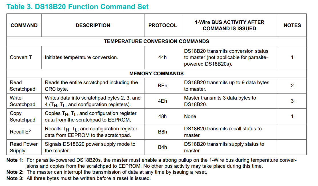
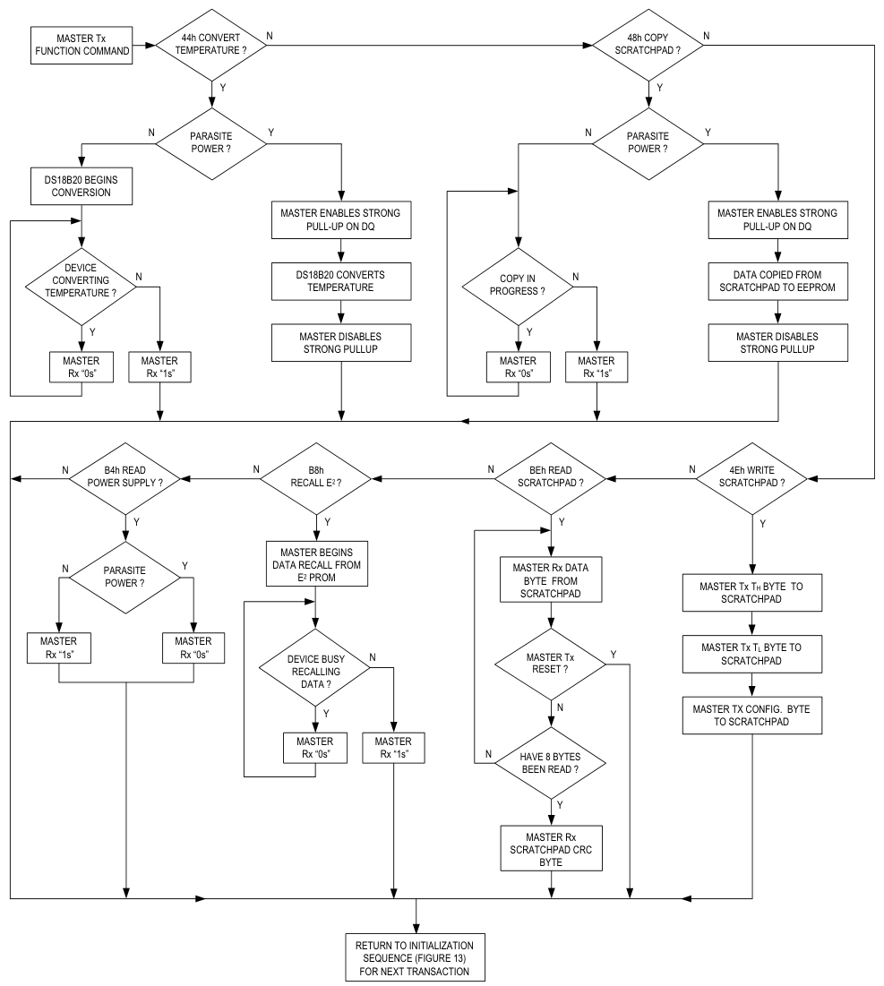
Convert T [44h]
This command starts a temperature measurement.
After the conversion is complete:
- The temperature result is written to the 2-byte temperature register in the scratchpad.
- The chip enters a low-power idle state.
If in parasitic power mode:
- Within 10µs after the host sends the command
- must enable strong pull-up
- for the entire conversion time tCONV
If in external power mode:
The host can continuously read time slots:
- Returns 0 → still converting
- Returns 1 → conversion complete
In parasitic power mode, you cannot query this way because the bus is strongly pulled up.
Write Scratchpad [4Eh]
Allows the host to write 3 bytes to the scratchpad:
- Byte 1 → TH (byte 2)
- Byte 2 → TL (byte 3)
- Byte 3 → configuration register (byte 4)
Data must:
- Low bit first (LSB first)
- The three bytes must be written completely before reset, otherwise data may be corrupted.
Read Scratchpad [BEh]
The host reads the scratchpad contents:
- Starting from the least significant bit of byte 0
- Read through to byte 8 (CRC)
If only partial data is needed:
- You can reset at any time to terminate the read.
Copy Scratchpad [48h]
The scratchpad’s:
12 | TH / TL / 配置寄存器(byte 2,3,4) |
Copy to EEPROM.
In parasitic power mode:
- Strong pull-up must be enabled within 10 µs.
- Must last at least 10 ms.
Recall E2 [B8h]
Read from EEPROM:
1 | TH / TL / 配置 |
Reload into the scratchpad.
The host can query the status:
- 0 → Restoring
- 1 → Complete
This operation is performed automatically at power-up, so the scratchpad has valid data as soon as power is applied.
Read Power Supply [B4h]
Detect power supply mode:
After the host sends a command, it reads a time slot:
- Bus pulled low → Parasitic power
- Bus held high → External power
Function Commands Timing Diagram
Operation Example
There is only one DS18B20 on the bus.
There is only one DS18B20 on the bus, and it uses parasitic power. The host writes TH, TL, and the configuration register to the DS18B20’s scratchpad, then reads the scratchpad and recalculates the CRC to verify the data. After that, the host copies the scratchpad contents to the EEPROM.
| Host Mode | Data (LSB first) | Description |
|---|---|---|
| Tx | Reset | Host sends reset pulse |
| Rx | Presence | DS18B20 returns presence pulse |
| Tx | CCh | Host sends Skip ROM (selects all devices on the bus) |
| Tx | 4Eh | Host sends Write Scratchpad |
| Tx | 3 bytes of data | Write TH, TL, and the configuration register |
| Tx | Reset | Host resets again |
| Rx | Presence | DS18B20 returns presence pulse |
| Tx | CCh | Skip ROM |
| Tx | BEh | Read Scratchpad |
| Rx | 9 bytes of data | Read scratchpad + CRC and verify |
| Tx | Reset | Host reset |
| Rx | Presence | DS18B20 returns presence pulse |
| Tx | CCh | Skip ROM |
| Tx | 48h | Copy Scratchpad |
| Tx | Strong pull-up ≥ 10ms | Strong pull-up power during EEPROM write |
Multiple DS18B20s on the 1-Wire bus
There are multiple DS18B20s on the bus, and they use parasitic power. The host initiates a temperature conversion for one specified DS18B20, then reads its scratchpad and recalculates the CRC to verify whether the data is correct.
| Host Mode | Data (LSB first) | Description |
|---|---|---|
| Tx | Reset | Host sends reset pulse |
| Rx | Presence | DS18B20 returns presence pulse |
| Tx | 55h | Host sends Match ROM command |
| Tx | 64-bit ROM code | Host specifies target DS18B20 |
| Tx | 44h | Host sends Convert T (start temperature conversion) |
| Tx | Strong pull-up held high | Host provides strong pull-up power during the entire conversion time tCONV |
| Tx | Reset | Host sends reset pulse again |
| Rx | Presence | DS18B20 returns presence pulse |
| Tx | 55h | Host sends Match ROM again |
| Tx | 64-bit ROM code | Select the same device again |
| Tx | BEh | Host sends Read Scratchpad |
| Rx | 9 bytes of data | The host reads the scratchpad (including CRC) and calculates the CRC check by itself. |
Communication Timing
DS18B20 uses a strict 1-Wire communication protocol to ensure data integrity. This protocol defines several signal types:
reset pulsepresence pulsewrite 0write 1read 0read 1
On the 1-Wire bus, all data is LSB first (least significant bit first).
Reset timing
1-WireAll communication on the bus uses a Initialization sequence Start.
This initialization sequence includes:
- one sent by the host reset pulse
- Subsequently sent by the slave device presence pulse
The function of the presence pulse is to tell the host that there are slave devices (e.g., DS18B20) on the bus and they are ready to communicate.

During initialization:
- The host sends a reset pulse, pulling the 1-Wire bus low. At least 480µs
- The host releases the bus and enters receive mode. After release, the bus is pulled high by a 5kΩ pull-up resistor.
- DS18B20 detects a rising edge and waits 15µs ~ 60µs
- DS18B20 sends a presence pulse, pulling the bus low. 60µs ~ 240µs
- The bus is pulled high by a pull-up resistor (RESISTOR PULLUP)
Read/Write Timing
- The main unit is here Write slot In the slot, write data to DS18B20,
- Before Read slot In the slot, read data from DS18B20.
On the 1-Wire bus: each time slot transmits only 1 bit of data.

Write Time Slots
There are two types of write slots:
- Write 1
- Write 0
The host uses: Write 1 slot to write logic 1, Write 0 slot to write logic 0

All write slots must satisfy:
- Each time slot ≥ 60µs and ≤ 120µs
- Recovery time between adjacent time slots ≥ 1µs
Both types of write slots are started by the host: first pulling the 1-Wire bus low
Write 1 rule
After the host pulls the bus low: it must release it within 15µs
After release: the 5kΩ pull-up resistor will pull the bus high
Write 0 rule
- After the host pulls the bus low: it must hold it low for ≥ 60µs
DS18B20 will detect the bus state in a sampling window: after the host starts the write slot, 15µs ~ 60µs between, if during this time:
- Bus is high → write 1
- Bus is low → write 0
Read Time Slots
DS18B20 Data can only be sent in read slots. So:
- If the host wants to read data, it must actively create read slots
- The slave cannot speak on its own.
This is a type of:master-driven synchronous communication
The master reads immediately after these commands:
- Read Scratchpad [BEh]
- Read Power Supply [B4h]
In addition, the status can be queried using read slots:
- Convert T [44h] (whether temperature conversion is complete)
- Recall E2 [B8h]

Read slots are initiated by the master:
- Master pulls the bus low ≥ 1µs
- Master releases the bus
- DS18B20 sends 0 or 1 in this window
- Send 1 → do nothing → line is pulled up → high level
- Send 0 → actively pull the bus low (DS18B20 releases the bus at the end of the slot, the pull-up resistor restores high level)
The entire Read Slot must be ≥ 60µs long,Recovery between slots ≥ 1µs
Therefore, DS18B20’s data is valid within 15µs after the start of the read slot, so the master must: complete sampling within 15µs

example
123456789101112131415161718192021222324252627282930313233343536373839404142434445464748495051525354555657585960616263646566676869707172737475767778798081828384858687888990919293949596979899100101102103104105106107108109110111112113114115116117118119120121122123124125126127128129130131132133134135136137138139140141142143144145146147148149150151152153154155156157158159160161162163164165166167168169170171172173174175176177178179180181182183184185186187188189190191192193194195196197198199200201202203204205206207208209210211212213214215216217218219220221222223224225226227228229230231232233234235236237238239240241242243244245246247248249250251252253254255256257258259260261262263264265266267268269270271272273274275276277278279280281282283284285286287288289290291292293294295296297298299300301302303304305306307308309310311312313314315316317318319320321322323324325326327328329330331332333334335336337338339340341342343344345346347348349350351352353354355356357358359360361362363364365366367368369370371372373374375376377378379380381382383384385386387388389390391392393394 | // ROM Command// Function Commandstruct ds18b20 { dev_t dev_num; struct cdev cdev; struct class *class; struct device *dev; struct gpio_desc *gpiod; struct fasync_struct *fa; u8 precision; // wait_queue_head_t wq;};int ds18b20_reset(struct gpio_desc *gpiod){ int timeout; // host send reset pulse gpiod_direction_output(gpiod, 0); udelay(500); // >= 480 us // host release the bus gpiod_direction_input(gpiod); udelay(60); // 15 us ~ 60 us // ds18b20 send presence pulse timeout = 240; while (gpiod_get_value(gpiod)) { // 60 us ~ 240 us if (timeout == 0) goto err; udelay(1); timeout--; } // resistor pullup timeout = 240; while (!gpiod_get_value(gpiod)) { // 60 us ~ 240 us if (timeout == 0) goto err; udelay(1); timeout--; } udelay(480); return 0;err: return -EIO;}void ds18b20_write_bit(struct gpio_desc *gpiod, char bit){ gpiod_direction_output(gpiod, 0); if (bit) { udelay(6); gpiod_direction_input(gpiod); udelay(80); // 60 ~ 120 } else { udelay(86); gpiod_direction_input(gpiod); } udelay(1);}void ds18b20_write_byte(struct gpio_desc *gpiod, char byte){ int i; for (i = 0; i < 8; i++) ds18b20_write_bit(gpiod, (byte >> i) & 0x1);}u8 ds18b20_read_bit(struct gpio_desc *gpiod){ char bit; gpiod_direction_output(gpiod, 0); udelay(2); // 1 us ~ 15 us, as smaller as possible gpiod_direction_input(gpiod); udelay(12); // wait for 12 us then read value bit = gpiod_get_value(gpiod); udelay(50); // >= 45us return bit;}u8 ds18b20_read_byte(struct gpio_desc *gpiod){ int i; char value = 0; for (i = 0; i < 8; i++) value |= ds18b20_read_bit(gpiod) << i; return value;}int ds18b20_open(struct inode *inode, struct file *file){ struct ds18b20 *drv_data = container_of(inode->i_cdev, struct ds18b20, cdev); //struct gpio_desc *gpiod = drv_data->gpiod; file->private_data = drv_data; // Precision set to 12 drv_data->precision = 12; pr_info("%s success, default precision is %d\n", __func__, drv_data->precision); return 0;}int ds18b20_release(struct inode *inode, struct file *file){ pr_info("%s\n", __func__); return 0;}ssize_t ds18b20_read(struct file *file, char __user *buf, size_t size, loff_t *offset){ char ls_byte, ms_byte; struct ds18b20 *drv_data = file->private_data; struct gpio_desc *gpiod = drv_data->gpiod; int16_t raw_temp; size_t count = min(sizeof(int16_t), size); int ret; // Reset ret = ds18b20_reset(gpiod); if (ret < 0) { pr_err("%s: reset fail\n", __func__); return ret; } // Only one DS18B20, send Skip ROM ds18b20_write_byte(gpiod, ROM_CMD_SKIP_ROM); // Function Command, send Convert T ds18b20_write_byte(gpiod, FUNC_CMD_CONVERT_T); switch (drv_data->precision) { case 12: msleep(750); break; case 11: msleep(375); break; case 10: msleep(188); break; case 9: msleep(94); break; default: pr_err("unsupported precision\n"); return -EFAULT; } // Reset ret = ds18b20_reset(gpiod); if (ret < 0) { pr_err("%s: reset fail\n", __func__); return ret; } // Only one DS18B20, send Skip ROM ds18b20_write_byte(gpiod, ROM_CMD_SKIP_ROM); // Function Command, send Read Scratchpad ds18b20_write_byte(gpiod, FUNC_CMD_READ_SCRATCHPAD); // read val ls_byte = ds18b20_read_byte(gpiod); ms_byte = ds18b20_read_byte(gpiod); raw_temp = (int16_t)(((u16)ms_byte << 8) | ls_byte); pr_info("raw_temp is %d\n", raw_temp); if (copy_to_user(buf, &raw_temp, count) != 0) return -EFAULT; // TODO CRC return count;}long ds18b20_unlocked_ioctl(struct file *file, unsigned int cmd, unsigned long arg){ char ls_byte, ms_byte; struct ds18b20 *drv_data = file->private_data; struct gpio_desc *gpiod = drv_data->gpiod; int16_t raw_temp; int ret; switch (cmd) { case DS_CMD_START: // Reset ret = ds18b20_reset(gpiod); if (ret < 0) { pr_err("%s: ds18b20 reset failed\n", __func__); return ret; } // Only one DS18B20, send Skip ROM ds18b20_write_byte(gpiod, ROM_CMD_SKIP_ROM); // Function Command, send Convert T ds18b20_write_byte(gpiod, FUNC_CMD_CONVERT_T); switch (drv_data->precision) { case 12: msleep(750); break; case 11: msleep(375); break; case 10: msleep(188); break; case 9: msleep(94); break; default: pr_err("unsupported precision\n"); return -EFAULT; } break; case DS_CMD_SET_PREC: break; case DS_CMD_GET_TEMP: // Reset ret = ds18b20_reset(gpiod); if (ret < 0) { pr_err("%s: reset fail\n", __func__); return ret; } // Only one DS18B20, send Skip ROM ds18b20_write_byte(gpiod, ROM_CMD_SKIP_ROM); // Function Command, send Read Scratchpad ds18b20_write_byte(gpiod, FUNC_CMD_READ_SCRATCHPAD); // read val ls_byte = ds18b20_read_byte(gpiod); ms_byte = ds18b20_read_byte(gpiod); raw_temp = (int16_t)(((u16)ms_byte << 8) | ls_byte); pr_info("raw_temp is %d\n", raw_temp); // if (copy_to_user((void *)arg, &raw_temp, sizeof(int16_t)) != 0) // return -EFAULT; if(put_user(raw_temp, (int16_t __user *)arg)) return -EFAULT; break; default: pr_err("unknown ioctl cmd\n"); return -EFAULT; } return 0;}int ds18b20_fasync(int fd, struct file *file, int on){ struct ds18b20 *drv_data = file->private_data; return fasync_helper(fd, file, on, &drv_data->fa);}struct file_operations ds18b20_fops = { .owner = THIS_MODULE, .open = ds18b20_open, .release = ds18b20_release, .read = ds18b20_read, .llseek = no_llseek, .unlocked_ioctl = ds18b20_unlocked_ioctl,};static int ds18b20_probe(struct platform_device *pdev){ int ret; //struct device *dev = &pdev->dev; struct ds18b20 *ds18b20; ds18b20 = kzalloc(sizeof(*ds18b20), GFP_KERNEL); if (!ds18b20) { ret = -ENOMEM; goto err_kzalloc; } ret = alloc_chrdev_region(&ds18b20->dev_num, 0, 1, "ds18b20"); if (ret < 0) goto err_chrdev_region; cdev_init(&ds18b20->cdev, &ds18b20_fops); ds18b20->cdev.owner = THIS_MODULE; ret = cdev_add(&ds18b20->cdev, ds18b20->dev_num, 1); if (ret < 0) goto err_cdev; ds18b20->class = class_create(THIS_MODULE, "one-wire"); if (IS_ERR(ds18b20->class)) { ret = PTR_ERR(ds18b20->class); goto err_class; } // /sys/class/one-wire/ds18b20 ds18b20->dev = device_create(ds18b20->class, NULL, ds18b20->dev_num, NULL, "ds18b20"); if (IS_ERR(ds18b20->dev)) { ret = PTR_ERR(ds18b20->dev); goto err_device_create; } ds18b20->gpiod = gpiod_get_optional(&pdev->dev, "ds18b20", GPIOD_OUT_HIGH); if (IS_ERR_OR_NULL(ds18b20->gpiod)) { if (ds18b20->gpiod == NULL) ret = -ENODEV; else if (IS_ERR(ds18b20->gpiod)) ret = PTR_ERR(ds18b20->gpiod); goto err_get_gpio; } platform_set_drvdata(pdev, ds18b20); return 0;err_get_gpio: device_destroy(ds18b20->class, ds18b20->dev_num);err_device_create: class_destroy(ds18b20->class);err_class: cdev_del(&ds18b20->cdev);err_cdev: unregister_chrdev_region(ds18b20->dev_num, 1);err_chrdev_region: kfree(ds18b20);err_kzalloc: return ret;}static int ds18b20_remove(struct platform_device *pdev){ struct ds18b20 *ds18b20 = platform_get_drvdata(pdev); gpiod_put(ds18b20->gpiod); device_destroy(ds18b20->class, ds18b20->dev_num); cdev_del(&ds18b20->cdev); class_destroy(ds18b20->class); unregister_chrdev_region(ds18b20->dev_num, 1); kfree(ds18b20); return 0;}const struct of_device_id match_table[] = { { .compatible = "even629,ds18b20" },};struct platform_driver ds18b20_pdrv = { .driver = { .name = "ds18b20", .owner = THIS_MODULE, .of_match_table = match_table, }, .probe = ds18b20_probe, .remove = ds18b20_remove,};module_platform_driver(ds18b20_pdrv);MODULE_LICENSE("GPL");MODULE_AUTHOR("even629<asqwgo@outlook.com>");MODULE_DESCRIPTION("This is a test sample for ds18b20"); |