
Timeline
Timeline
2025-10-30
init
This article introduces the ARM NEON instruction set and its related technical details, focusing on the concepts of vector registers and lanes, including registers of different bit widths such as Vn, Dn, Sn, Hn, Bn and their corresponding vector group representation methods, and explains how to index specific data values in lanes. The article also elaborates on the representation and operations of floating-point numbers under the ARMv8 architecture, including the storage formats of single-precision and double-precision floating-point numbers, IEEE 754 standard support, and demonstrates the steps of converting decimal numbers to binary floating-point numbers through specific examples. In addition, the article summarizes the roles of key control bits in the FPCR register, such as the AHP bit controlling whether half-precision floating-point uses the IEEE standard or an ARM alternative implementation, the DN bit controlling the default NaN mode, and compares the differences between two half-precision floating-point formats in the representation of infinity and NaN. The overall content covers the basic data structures of NEON instructions, floating-point operation principles, and control register configuration, providing a reference for understanding SIMD and floating-point operations in ARM processors.
Reference documents:

Floating-point operations
Floating-point operations (FP) and NEON instructions
- VFP development history
- VFPv1: Early version
- VFPv2: VFP coprocessor in ARMv5 and ARMv6 processors
- VFPv3: ARMv7 processors
- VFPv4: ARMv7 processors
- NEON: Supports SIMD instructions and floating-point instructions
Vector registers and lanes

- A vector is divided into multiple lanes, each lane contains a vector element.

- Lane data types:
- Vn: 128-bit data type
- Dn: 64-bit data type
- Sn: 32-bit data type
- Hn: 16-bit data type
- Bn: 8-bit data type
| Name | Bit width | Corresponding V register range | Description |
|---|---|---|---|
| Vn | 128 bit | V0–V31 | NEON 128-bit register (full vector) |
| Dn | 64 bit | D0–D31 | Lower 64 bits of Vn (Double precision) |
| Sn | 32 bit | S0–S31 | Lower 32 bits of Dn (Single precision) |
| Hn | 16 bit | H0–H31 | Next level below S register (Half precision) |
| Bn | 8 bit | B0–B31 | Least significant 8 bits (Byte) |


| Vector group representation method | meaning |
|---|---|
| Vn.8B | 8 bits × 8 lanes, representing 8 data channels, each data element being 8 bits of data. |
| Vn.4H | 16 bits × 4 lanes, representing 4 data channels, each data element being 16 bits of data. |
| Vn.2S | 32 bits × 2 lanes, representing 2 data channels, each data element being 32 bits of data. |
| Vn.1D | 64 bits × 1 lane, representing 1 data channel, each data element being 64 bits of data. |
| Vn.16B | 8 bits × 16 lanes, representing 16 data channels, each data element being 8 bits of data. |
| Vn.4S | 32 bits × 4 lanes, representing 4 data channels, each data element being 32 bits of data. |
| Vn.2D | 64 bits × 2 lanes, representing 2 data channels, each data element being 64 bits of data. |
Index the value of a channel
- For example, “V0.S[1]” represents the 32-bit data at index 1 in the V0 vector group, i.e., Bit[63:32].
Vector register list

Vector register list Index the value of a channel in the vector register list

Index the value of a channel in the vector register list
Floating-point numbers
- ARMv8 supports the IEEE 754 standard.
- ARM64 processors support single-precision and double-precision floating-point numbers. In ARM64 processors, single-precision floating-point numbers are represented by 32-bit Sn registers, and double-precision floating-point numbers are represented by 64-bit Dn registers.
- In C, the float type can be used to represent single-precision floating-point numbers, and the double type to represent double-precision floating-point numbers.
- A floating-point number consists of three parts: sign bit S, exponent, and mantissa.
- A sign bit of 0 indicates a positive number, and 1 indicates a negative number.
- The exponent has a fixed bias of 127.
- A single-precision floating-point number uses 32 bits of space, with an 8-bit exponent and a 24-bit mantissa.
- A double-precision floating-point number uses 64 bits of space, with an 11-bit exponent and a 53-bit mantissa.

Binary representation of floating-point numbers
Convert the decimal number (5.25) to a single-precision floating-point number. What is its binary storage format?
Step
- To convert a decimal number to a binary number: convert the integer part directly to a binary number, and for the fractional part, multiply by 2 and take the integer digit.
For the integer part, directly convert 5 to binary, resulting in the binary number: 101
For the fractional part, multiply the decimal fractional part by 2, and use the digit to the left of the decimal point (0 or 1) of the product as a digit in the binary representation, until the required precision is reached.
0.25 * 2 = 0.5, the digit to the left of the decimal point is 0
0.5 * 2 = 1.0, the digit to the left of the decimal point is 1
The decimal number (5.25) converted to binary is 101.01
- Normalize the binary number by changing the exponent so that there is only one significant digit before the decimal point.
After normalization, the binary number (101.01) becomes: 1.0101 * 2^2, where the mantissa is 0101 and the exponent is 2.
- Calculate the exponent. For single-precision floating-point numbers, add the bias of 7F (127); for double-precision floating-point numbers, add the bias of 3FF (1023).
In this example, the final exponent is 129
- Combine the sign bit, exponent, and mantissa to obtain the floating-point storage format.
In this example, the sign bit is 0, the exponent is: 1000 0001, the mantissa is: 0101, expressed in hexadecimal as: 0x40a80000
Experiment 1: Binary representation of floating-point numbers

fmov instruction
The floating-point constants supported by the fmov instruction are limited.

FPCR register
Floating-point Control Register

AHP (bit 26) — Alternative half-precision control bit
This flag bit is used to control whether half-precision floating-point uses the IEEE 754-2008 standard or an alternative implementation designed by ARM. When this flag is 0, the half-precision representation of the IEEE 754-2008 standard is used; when it is 1, the alternative representation designed by ARM is used.
It should be noted here that the FP16 instruction extension introduced from ARMv8.2 directly uses the IEEE format for half-precision floating-point and ignores this flag.
The following briefly introduces ARM’s own half-precision floating-point representation. It is described in detail in Section A1.4.2 (Half-precision floating-point formats) of the ARMv8 Reference Guide. Like the IEEE 754-2008 specification, it has 1 sign bit, 5 exponent bits, and 10 mantissa bits. However, the two representations differ in representing infinity and NaN.

When the exponent field is all 1s (i.e., 0x1F):
- For IEEE754-2008: this half-precision floating-point number may be positive or negative infinity (±∞, ±INF), or it may be a NaN. It depends on the mantissa field — if the mantissa field is all zeros, then when the sign bit S=0, the floating-point number is +INF; when S=1, it is -INF. If the mantissa field is not zero, then look at the most significant bit of the mantissa (bit 9); if it is 0, the NaN is an SNaN; otherwise it is a QNaN.
- For the ARM alternative implementation of half-precision floating-point: the floating-point value is treated as a normalized number, equivalent to (-1)^S × 2^16 × (1.fraction). This means the maximum positive normalized number is (2 - 2^-10) × 2^16 = 131008.
DN (bit 25) — Default NaN mode control bit
This flag controls whether a NaN operand is propagated to the output of a floating-point operation, i.e., even if an operand is NaN, the computation is still fully executed. If this flag is set to 1, then for a floating-point operation instruction, as long as any operand is NaN, a default NaN value set by the ARM processor is returned immediately. This flag can also improve floating-point execution performance.
If the DN flag is 1, the default NaN values for the three floating-point types are as follows:
- 16-bit half-precision floating-point: 0x7E00
- 32-bit single-precision floating-point: 0x7FC0’0000
- 64-bit double-precision floating-point: 0x7FF8’0000’0000’0000
FZ (bit 24) — Flush-to-zero mode control bit
The behavior of this mode is consistent with the DAZ flag on x86 (rather than FTZ) — if this flag is set to 1, then for a floating-point computation instruction, all denormalized numbers in the operands are rounded to 0. In addition, this flag only controls 32-bit single-precision and 64-bit double-precision floating-point, and does not affect the 16-bit half-precision floating-point introduced by ARMv8.2-FP16.
RMode (bits 23:22) — Rounding Mode control field
This field pertains to the rounding mode of floating-point numbers.
FZ16 (bit 19) — Flush-to-zero mode control bit on half-precision data-processing instructions
This flag is only valid when the ARM architecture supports the ARMv8.2-FP16 instruction extension. This flag controls the flush-to-zero operation for half-precision floating-point, with the same semantics as FZ above. However, this flag is only used to control 16-bit half-precision floating-point and does not affect other floating-point types.
Architectural Feature Access Control Register CPACR_EL1
Fields that control whether FP/NEON register accesses trap to EL1:FPEN
- When FPEN is 0b01, it means that accesses to SVE, Advanced SIMD, and floating-point unit registers in EL0 will trap to EL1 for handling, with exception type code 0x7.
- When FPEN is 0b00 or 0b10, it means that accesses to SVE, Advanced SIMD, and floating-point unit registers in EL0 or EL1 will trap to EL1 for handling, with exception type code 0x7.
- When FPEN is 0b11, it means no trap to EL1 occurs.
Floating-point condition codes
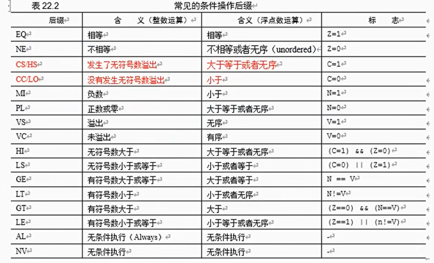
Common floating-point instructions
- Instructions beginning with the letter F, about several dozen instructions.
- See Chapter C.2 of the ARMv8.6 manual.
- See the ARM Compiler arm asm User Guide, v6.6, Chapters 18-20

NEON instruction optimization
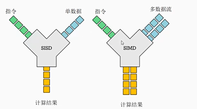
SISD and SIMD
- SISD (Single Instruction Single Data) refers toSingle instruction, single data。Each instruction performs its specified operation on a single data source
1234 | ADD w0, w0, w5ADD w1, w1, w6ADD w2, w2, w7ADD w3, w3, w8 |
- SIMD refers toSingle instruction, multiple data, whichPerforms the same operation on multiple data elements simultaneouslyThese data elements are packed into independent lanes in a larger register.

LD1 instruction
The LD1 instruction is used to load multiple elements into one, two, three, or four vector registers.
The LD1 instruction supportsno offsetandpost-indextwo modes
- no-offset mode
1234
LD1 {<Vt>.<T> }, [<Xn|SP>]LD1 {<Vt>.<T>, <Vt2>.<T>}, [<Xn|SP>]LD1 {<Vt>.<T>, <Vt2>.<T>, <Vt3>.<T>}, [<Xn|SP>]LD1 {<Vt>.<T>, <Vt2>.<T>, <Vt3>.<T>, <Vt4>.<T>}, [<Xn|SP>]

LD1 instruction encoding - Post-index mode
1234
LD1 {<Vt>.<T> }, [<Xn|SP>], <imm>LD1 {<Vt>.<T>, <Vt2>.<T>}, [<Xn|SP>], <imm>LD1 {<Vt>.<T>, <Vt2>.<T>, <Vt3>.<T>}, [<Xn|SP>], <imm>LD1 {<Vt>.<T>, <Vt2>.<T>, <Vt3>.<T>, <Vt4>.<T>}, [<Xn|SP>], <imm>
Example 1: LD1 instruction loads RGB24
- Taking the RGB24 image format as an example, a pixel uses 24 bits (3 bytes) to represent three colors: R (red), G (green), and B (blue). Their storage format in memory is R0, G0, B0, R1, G1, B1, and so on.

- Use the LD1 instruction to load RGB24 format data into vector registers
1 | LD1 {V0.16B, V1.16B, V2.16B}, [x0] |

ST1 instruction
The ST1 instruction stores the contents of multiple data elements from one, two, three, or four vector registers to memory.
The ST1 instruction supports no-offset and post-index modes.
- No offset mode:
1234
ST1 {<Vt>.<T>}, [<Xn|SP>]ST1 {<Vt>.<T>,<Vt2>.<T>},[<Xn|SP>]ST1 {<Vt>.<T>,<Vt2>.<T>,<Vt3>.<T>},[<Xn|SP>]ST1 {<Vt>.<T>,<Vt2>.<T>,<Vt3>.<T>,<Vt4>.<T>},[<Xn|SP>]
- Post-index mode:
1234
ST1 {<Vt>.<T>}, [<Xn|SP>], <imm>ST1 {<Vt>.<T>,<Vt2>.<T>},[<Xn|SP>], <imm>ST1 {<Vt>.<T>,<Vt2>.<T>,<Vt3>.<T>},[<Xn|SP>], <imm>ST1 {<Vt>.<T>,<Vt2>.<T>,<Vt3>.<T>,<Vt4>.<T>},[<Xn|SP>], <imm>
Example: ST1 instruction stores RGB24
- V0, V1, and V2 vector registers store data in RGB24 format, and the ST1 instruction is used to store the data to memory.
1 | ST1 {V0.16B, V1.16B, V2.16B}, [x0] |

Experiment 2: Using LD1 and ST1 instructions


LD2/ST2: Interleave load and store
The LD2 and ST2 instructions support loading and storing data in an interleaved manner.
Supports two modes: no offset and post-indexed.
12345
LD2 {<Vt>.<T>,<Vt2>.<T>},[<Xn|SP>]ST2 {<Vt>.<T>,<Vt2>.<T>},[<Xn|SP>]LD2 {<Vt>.<T>,<Vt2>.<T>},[<Xn|SP>], <imm>ST2 {<Vt>.<T>,<Vt2>.<T>},[<Xn|SP>], <imm>
Example
1 | LD2 {V0.8H, V1.8H}, [x0] |

Experiment 3: Using LD2 and ST2 instructions

LD3/ST3: Three-channel interleave
- In RGB24 to BGR24 conversion, if we use the LD1 instruction to load RGB24 data into vector registers, we need to obtain different color components from different channels, then move and recombine these components, which is very inefficient.
- The LD3 and ST3 instructions support loading and storing data in an interleaved manner.
- Supports two modes: no offset and post-indexed.
12345 | LD3 {<Vt>.<T>, <Vt2>.<T>, <Vt3>.<T>}, [<Xn|SP>]ST3 {<Vt>.<T>, <Vt2>.<T>, <Vt3>.<T>}, [<Xn|SP>]LD3 {<Vt>.<T>, <Vt2>.<T>, <Vt3>.<T>}, [<Xn|SP>], <imm>ST3 {<Vt>.<T>, <Vt2>.<T>, <Vt3>.<T>}, [<Xn|SP>], <imm> |
Example: RGB24 to BGR24
- Use the LD3 instruction to load RGB24 format data into vector registers.
1 | LD3 {V0.16B, V1.16B, V2.16B}, [x0] |


Store RGB24 to memory

Experiment 4: Using LD3/ST3 to implement RGB24 to BGR24 conversion

C language implementation

Assembly implementation

LD4/ST4: Four-channel interleave
- ARGB images are based on RGB with an added Alpha (transparency) channel. To speed up data loading and storage operations for the ARGB format, the NEON instructions provide LD4 and ST4 instructions. LD4 is similar to LD3, but it can de-interleave data and load it into four vector registers.
- The LD4 and ST4 instructions support loading and storing data in an interleaved manner.
- Supports two modes: no offset and post-indexed.
12345 | LD4 {<Vt>.<T>,<Vt2>.<T>,<Vt3>.<T>,<Vt4>.<T>},[<Xn|SP>]ST4 {<Vt>.<T>,<Vt2>.<T>,<Vt3>.<T>,<Vt4>.<T>},[<Xn|SP>]LD4 {<Vt>.<T>,<Vt2>.<T>,<Vt3>.<T>,<Vt4>.<T>},[<Xn|SP>], <imm>ST4 {<Vt>.<T>,<Vt2>.<T>,<Vt3>.<T>,<Vt4>.<T>},[<Xn|SP>], <imm> |
LDnR instruction
- The LDn instruction also has a variant, the LDnR instruction,**R stands for repeat.**It loads a group of data elements from memory, then copies each element to all lanes of the corresponding vector register.
- Example:
1 | LD3R {V0.16B, V1.16B, V2.16B}, [x0] |

Read and write the value of a specific lane.
- The LDn instruction can load data into a specific lane of a vector register while the values of other lanes remain unchanged.
- Example:
1 | LD3 {V0.B, V1.B, V2.B}[4], [x0] |

MOV instruction
- Move data from general-purpose registers.
12 | mov w1, #0xamov v1.h[2], w1 |
- Vector register move
12 | MOV V3.16B, V0.16BMOV V3.8B, V0.8B |
- Move data elements to a vector register.
1 | mov h2, v1.8h[2] |
- Move data elements.
1 | mov v1.8h[2], v0.8h[2] |
MOVI
movi is in the ARMv8 (AArch64) architecture **A vector immediate load instruction of NEON (Advanced SIMD).
Its full name is “Move Immediate (vector)”。
moviUsed for:
Move animmediate value Load into a SIMD/floating-point register (Vn or Qn) Middle.
It can fill all elements in a register at once, often used to initialize vector registers.
Syntax format
There are several common forms (using A64 assembly as an example):
123 | movi Vd.<T>, #immmovi Vd.<T>, #imm, LSL #shiftmovi Vd.<T>, #imm, MSL #shift |
Where:
Vd: destination register (e.g.,v0、v1)<T>: data type (such as8b、16b、4h、2s、1detc.)#imm: immediate valueLSL/MSL: logical left shift / sign-extended left shift, used to change the immediate value filling rules
Reverse instructions
- REV16 instruction
Indicates that 16-bit data elements in a vector register form a container. Within this 16-bit container, reverse the order of 8-bit data elements, i.e., reverse the order between B[0] and B[1].
- REV32 instruction
Indicates that 32-bit data elements in a vector register form a container. Within this container, reverse the order of 8-bit or 16-bit data elements.
- REV64 instruction
Indicates that 64-bit data elements in a vector register form a container. Within this container, reverse the order of 8-bit, 16-bit, or 32-bit data elements.
Example 1:
1 | REV16 V0.16B, V1.16B |
V0 is the destination register, V1 is the source register

Example 2:
1 | REV32 V0.16B, V1.16B |

Example 3:
1 | REV64 V0.16B, V1.16B |

ZIP1 and ZIP2 instructions
- The ZIP1 instruction extracts half of the data elements from each of the two source vector registers, then interleaves them to form a new vector, which is written to the destination vector register.
- The ZIP2 instruction extracts half of the data elements from each of the two source vector registers, where it extracts from the source vector registershigh partdata elements, then interleaved to form a new vector, written to the destination vector register
Example:
12 | ZIP1 V0.8H, V3.8H, V4.8HZIP2 V1.8H, V3.8H, V4.8H |

TRN1 and TRN2 interleaved exchange instructions
- The TRN1 instruction extracts odd-indexed data elements from two source vector registers in an interleaved manner to form a new vector, and writes it to the destination vector register
- The TRN2 instruction extracts even-indexed data elements from two source vector registers in an interleaved manner to form a new vector, and writes it to the destination vector register
Example
1 | TRN1 V1.4S, V0.4S, V3.4S |

1 | TRN2 V2.4S, V0.4S, V3.4S |

TBL table lookup instruction
- The TBL instruction format is as follows

Example:
1 | TBL V4.16B, {V1.16B, V2.16B}, V0.16B |

There is also a variant instruction TBX; the only difference is that when the index is out of bounds, it retains the original value instead of writing 0
Multiply-accumulate instruction MLA
- The MLA instruction is a multiply-accumulate instruction: Vd += Vn * Vm
- Example
1 | mla v2.4s, v0.4s, v1.4s |

This full-vector form supports element sizes such as b, h, and s
1 | mla v2.4s, v0.4s, v1.4s[0] |

This scalar-index form supports h and s, but not b
Experiment 5: Familiarize with the MLA instruction

12345678910111213141516171819202122232425262728 | neon_mla_test: stp x29, x30, [sp, -16]! movi v3.16b, 0 movi v4.16b, 0 // Read 16 consecutive bytes from the address in x0 into v0.16b ld1 {v0.16b}, [x0], 16 ld1 {v1.16b}, [x0], 16 mla v3.16b, v0.16b, v1.16b mla v3.16b, v0.16b, v1.16b mov w1, #0 mov v2.4s[0], w1 mov w1, #1 mov v2.4s[1], w1 mov w1, #2 mov v2.4s[2], w1 mov w1, #3 mov v2.4s[3], w1 mov w1, #4 mov v5.4s[0], w1 mov w1, #5 mov v5.4s[1], w1 mla v4.4s, v2.4s, v5.4s[0] mla v4.4s, v2.4s, v5.4s[1] ldp x29, x30, [sp], 16 ret |
Vector arithmetic instructions

Experiment 6: Case Study 1 - RGB24 to BGR24
C language implementation

Inline assembly

Note two points:
- Using post-indexed addressing mode, so dst and src should be placed in the output section
- In the clobber section, tell the compiler that the four vector registers v0, v1, v2, v3 are used; otherwise, the compiler may allocate these vector registers elsewhere.
Using NEON intrinsics
Some NEON instructions encapsulated by the compiler

Document:
- 《Arm Neon Intrinsics Reference for ACLE Q3 2020》
- 《NEON Programmer Guide》
4×4 matrix multiplication

C language implementation

Handwritten NEON assembly

Using NEON intrinsics


Automatic vectorization
- There are three ways to optimize code using the NEON instruction set, as follows:
- Handwritten NEON assembly code
- Use the NEON intrinsics provided by the compiler
- Use the compiler’s auto-vectorization option to let the compiler automatically generate NEON instructions for optimization
- The GCC compiler has built-in auto-vectorization functionality. GCC provides the following compilation options:
- -ftree-vectorize: Perform vectorization. This enables “-ftree-loop-vectorize” and “-ftree-slp-vectorize” by default.
- -ftree-loop-vectorize: Perform loop vectorization. Unroll loops to reduce the number of iterations while performing more operations in each iteration.
- -ftree-slp-vectorize: Bundle scalar operations together to utilize the bandwidth of vector registers. SLP is an abbreviation for Superword-Level Parallelism.
- GCC’s “O3” optimization option automatically enables “-ftree-vectorize”, i.e., enables the auto-vectorization functionality.
Auto-vectorization constraints
- GCC’s auto-vectorization functionality may not work in some cases.
- In iterations of different loops that have dependencies on each other
- Loops with break statements
- Loops with complex conditions