
Timeline
Timeline
2025-10-26
init
This article introduces memory ordering and memory barrier mechanisms in the ARMv8 architecture. It first explains the weak consistency memory model and its causes, pointing out that hardware reordering may lead to inconsistent ordering of data accesses across multiple cores. It then details the data memory barrier (DMB), data synchronization barrier (DSB), and instruction synchronization barrier (ISB) instructions provided by ARMv8, focusing on the difference between DMB and DSB: DMB only guarantees ordering of data accesses, while DSB requires all previous data accesses and operations such as cache and TLB to complete before subsequent instructions execute. In addition, the article explains the Shareability domain parameter of barrier instructions and the configuration of read/write type (LD/ST) suffixes, and lists typical scenarios requiring memory barriers, such as multi-core shared data, DMA operations, and self-modifying code.
Reference documents:

ARMv8.6 Chip Manual
- Section B2.3.7 Memory barriers
- Appendix K11 Barrier Litmus Tests
Reasons for memory barriers
The ARMv8 architecture uses a weakly ordered memory model. In general, this means that the order of memory accesses does not need to be the same as the program order of load and store operations. The processor can reorder memory read operations relative to one another. Writes can also be reordered (for example, write combining). Hardware optimizations (such as the use of caches and write buffers) therefore operate in a way that improves processor performance, which means that the required bandwidth can be reduced, the latency between the processor and external memory can be reduced, and long latencies associated with such external memory accesses can be hidden.
Reads and writes to normal memory can be reordered by hardware, subject only to data dependencies and explicit memory barrier instructions. Some situations require stricter ordering rules.
- Processors use superscalar techniques: out-of-order issue, out-of-order execution, to increase instruction-level parallelism.

The order of these two statements is indeterminate because there is no dependency between them.
Memory consistency model
- Atomic consistency memory model
- Sequential consistency memory model
- Processor consistency memory model
- Weak consistency memory model
Compiler reordering
Weak consistency memory model
- In 1986, a paper by Dubois et al. described the definition of the weak consistency memory model.
- The weak consistency memory model requires that synchronization accesses (accesses to global synchronization variables) are sequentially consistent. Before a synchronization access can be performed, all previous data accesses must complete.
- Before a normal data access can be performed, all previous synchronization accesses must complete.
- Processors use memory barrier instructions to implement the overall synchronization access functionality.
- The basic principles of memory barrier instructions are as follows:
- All data accesses before the memory barrier instruction must complete before the memory barrier instruction.。
- All data accesses after the memory barrier instruction must wait for the memory barrier instruction to complete.。
- Multiple memory barrier instructions are executed in order.
- Memory barrier instructions can be parameterized by their scope (shareability domain).
Example

CPU0’s store operations may be reordered, and CPU1 may observe b=1 before observing a=1, so the assertion may fail.

ARMv8 memory model
Before normal memory on which is implementedweakly ordered memory model(weakly-ordered memory model)
Before device memory on which is implementedstrongly ordered memory model(strongly-ordered memory model)
The sequence of memory accesses may be inconsistent with the sequence in the code.
The ARMv8 architecture supports speculative accesses.
- Prefetch data or instructions from memory.
- Branch prediction
- Out-of-order data loads
- Speculative cache line fills
Speculative data accessesonly supports normal memory
Speculative prefetch of instructions can support any memory type.
In what situations do we need to consider memory barrier instructions?
- Sharing data between multiple different CPU cores (threads), such as mailbox, etc.
- Sharing data with peripherals, such as DMA operations.
- Modifying memory management policies, such as context switching, page faults, and modifying page tables.
- Modifying the memory region that stores instructions (instruction memory): for example, self-modifying code, loading a program into RAM.
Memory barrier instructions provided by ARMv8
- Data Memory BarrierData Memory Barrier (DMB) instruction
- Data Synchronization BarrierData Synchronization Barrier (DSB) instruction
- Instruction Synchronization Barrier(Instruction Synchronization Barrier, ISB) instruction
DMB instruction
Ordering of Load/Store instructions
- that only affects data accesses (explicit data accesses, such as load and store)access sequence
- Data cache maintenance instructions are also considered data accesses.
- guarantee thatdata accesses before DMBcan bedata access instructions after DMBobserved
DMBPoints to note about the instruction
- The DMB instruction focuses onthe sequence of memory accesses, and does not care when data access instructions complete execution
- Data access instructions before DMB must be observed by data access instructions after DMB.

- Data/unified cache instructions before DMB must complete execution (be observed) before the memory access instructions after DMB.

DSB instruction
Completion of Load/Store instructions
- The DSB instruction is much stricter than the DMB instruction.
- Beforeany instruction after the DSB instruction, must wait until the following is complete,before it can begin execution:
- before the DSB instructionall data accessesmust complete execution
- The cache, branch predictor, TLB, and other instructions before the DSB instruction must complete execution.
Things to note about the DSB instruction
- DMB instructionIt only concerns the ordering of data accesses., while the DSB instructionbegins to focus on when instructions must complete execution.
- Instructions after the DSB instruction must wait until:
- All data access instructions before the DSB have completed execution.
- All Cache, TLB, and other instructions before the DSB have completed execution.
The DSB instruction is more like a barrier.

- In amulti-core systemcache and TLB instructions are broadcast to other CPU cores, so the DSB instruction waits until these instructions are broadcast and acknowledgment signals from all cores are received before it completes.
The difference between DMB and DSB, example:


The ADD instruction is not a data access instruction.
Parameters of the DMB and DSB instructions
Two dimensions of parameters can be specified, one isShareability domain, the other isbefore-afteraccess
Shareability domain
- Full System
- Outer Shareable, prefix isOSH
- Inner Shareable, prefix isISH
- Non-shareable, prefix isNSH
before-after access (i.e., before and after the memory barrier instruction, further refined into read/write memory barriers)
Read barrier: Load-Load/Store: suffix isLD
This means that the barrier requires all loads to complete before the barrier but
does not require stores to complete. Both loads and stores that appear after the
barrier in program order must wait for the barrier to complete.Write barrier: Store-Store: suffix isST
This means that the barrier only affects store accesses and that loads can still be
freely re-ordered around the barrier.Read-write barrier: Any-Any: suffix isSY
This means that both loads and stores must complete before the barrier. Both
loads and stores that appear after the barrier in program order must wait for the
barrier to complete.

DMB and DSB instruction example 1: mailbox
- Two CPUs share data via mailbox: shared memory and flags

DMB and DSB instruction example 2: DMA peripheral

The DSB instruction ensures that the DMA engine sees the latest data already in the DMA buffer before starting.
Execution order of cache maintenance instructions
- Cache maintenance instructions (e.g., dc and ic) execute in the same order as other memory access instructions, with no special treatment.
- Instruction unit (instruction interface), data unit (data interface), MMU walker, etc., can be viewed as different observers.

Solution:

One-way memory barriers
Load-Acquire (LDAR)
All loads and stores that are after an LDAR in program order, and that match the shareability domain of the target address, must be observed after the LDAR.
Store-Release (STLR)
All loads and stores preceding an STLR that match the shareability domain of the target address, must be observed before the STLR.
There are also exclusive versions of the above, LDAXR and STLXR, available.
DMB and DSB are both bidirectional memory barrier instructions; ARMv8 also supports “one-way” memory barrier primitives.
Acquire primitive: refers toRead and write operations after the barrier primitive cannot be reordered before the barrier primitive., usually the barrier primitiveis combined with a load instruction
Release primitive: refers toRead and write operations before the barrier primitive cannot be reordered after the barrier primitive., usually the barrier primitivecombined with store instructions
Load-Acquire barrier primitive: ordinary read and write operations can pass backward over the barrier instruction, but subsequent read and write operations cannot pass forward over the barrier instruction
in ARMv8ldarInstruction

- Store-Release barrier primitive: ordinary read and write operations can pass forward over the store-release barrier instruction, but earlier read and write operations cannot pass backward over the store-release barrier instruction
- in ARMv8stlrInstruction

- Load-Acquire(Load-Acquire) andStore-Release(Store-Release) are usually used in pairs
- ldar and stlr Used in pairs:
- used to protect data in a critical section
- instructions in the critical section can be reordered (only within the critical section)
- has better performance than the full-featured DMB instruction
- has no effect on data cache maintenance instructions, because it does not wait for cache broadcasts

Instruction-level memory barrier instruction: ISB instruction
Context synchronization
The ISB instruction has a strong effect; it willflush the pipeline, thenrefetch instructions from the instruction cache or memory。
The ISB instruction ensures
- all instructions after ISB are refetched from the instruction cache or memory
- All context-changing operations before the ISB instruction have been completed (context here refers to system register state, etc.)
Context-changing operations include:
- Maintenance operations such as Cache, TLB, and branch predictor
- Changing system registers, e.g., TTBR0_EL1
The ARMv8 architecture defines context as the state of the system registers and context-changing operations as things like cache, TLB, and branch predictor maintenance operations, or changes to system control registers, for example, SCTLR_EL1, TCR_EL1, and TTBRn_EL1. The effect of such a context-changing operation is only guaranteed to be seen after a context synchronization event.
The effect of a context-changing operation: only aftera context synchronization eventcan it be observed
A context synchronization event (context synchronization event)
- taking an exception
- returning from an exception
- ISB instruction
In fact, after modifying system registers, an ISB instruction is generally required, especially when modifying system control registers (e.g., SCTLR_EL1、TCR_EL1, TTBRn_EL1), but not all system register modifications require ISB; modifications to some system registers (e.g., stack pointer SP) take effect for subsequent instructions without ISB.
ISB instruction example 1: Enabling the FPU

When changing a system control register, an ISB instruction is required
ISB instruction example 2: Changing page table entries

ISB instruction example 3: Self-modifying code
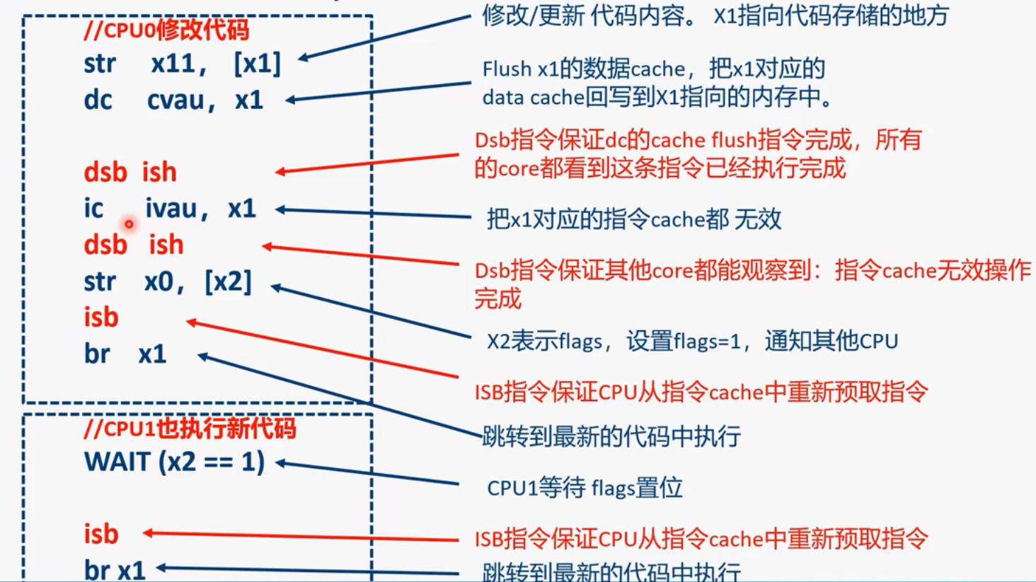
- No memory barrier instruction is used between updating the new code content (str x11, [x1]) and the clean data cache instruction
- Updating the code content and cleaning the data cache both operate on the same address, and both are data-related operations; there is a data dependency between them, so they can be understood as the same observer.
- Program order can be guaranteed between them
- A memory barrier is needed between cleaning the data cache and invalidating the instruction cache
- Although these two cache instructions operate on the same address, they are different observers (one is the data side, the other is the instruction side)
- The DSB here ensures that the instruction cache is invalidated only after the data cache has been cleaned
- In a multi-core coherent system, the DSB instruction can guarantee that cache maintenance instructions complete execution, that is, other CPUs can observe the completion of cache maintenance operations.
- The ISB instruction is not broadcast, so CPU1 also needs to execute the ISB instruction.
Non-temporal load and store pair
LDNP and STNP
LDNP and STNP are instructions that read or write a pair of register values. They also hint to the memory system that caching is of no use for this data. The hint does not prohibit memory system activities such as address caching, prefetching, or gathering, but merely indicates that caching is unlikely to improve performance. A typical use case might be streaming data, but it should be noted that effective use of these instructions requires a microarchitecture-specific approach.
**Non-temporal loads and stores relax memory ordering requirements.**Since the non-temporal hint of LDNP allows more relaxed ordering, it may be observed to execute before a previous ordinary load instruction, which could result in reading from an unpredictable address in X0. For example:
12 | LDR X0, [X3]LDNP X2, X1, [X0] |
To correct the above problem, you need an explicit load barrier instruction:
123 | LDR X0, [X3]DMB NSHLDLDNP X2, X1, [X0] |
Summary: Memory barrier instructions and cache/TLB maintenance instructions
- Data cache or unified cache maintenance instructions
- A DMB instruction can be used to ensure that cache maintenance instructions complete execution in the specified shareable domain.
- Load-acquire and store-release barriers have no effect on data cache maintenance instructions (because they do not wait for the cache broadcast).
- Instruction cache maintenance instructions
- From the perspective of memory observers, instruction cache and data cache are two different observers.
- Execute a DSB instruction after the instruction cache maintenance operation completes, ensuring that all CPU cores in the inner shareable domain can see the completion of the instruction cache maintenance operation.
- TLB maintenance instructions
- The unit that walks the page table and the hardware unit for data access are actually two different observers of the memory system.
- After a TLB maintenance instruction, a DSB instruction needs to be executed to ensure that all CPUs in the inner shareable domain can complete it.
- **The ISB instruction is not broadcast.**If each CPU core needs to observe the effects of a context change, each core must execute the ISB instruction separately.
Chip manual reading: memory barrier
ARM Architecture Reference Manual Armv8, for Armv8-A architecture profile
- B2.3.7 Memory barriers
- (Key points) Appendix K11 Barrier Litmus Test
ARM Cortex-A Series Programmer’s Guide for ARMv8-A
- 13.2 Barriers
Revisiting cache coherence and memory barriers
Problem introduction

The following execution order

CPU1’s assertion may still fail!!!
CPU stall caused by cache coherence protocol
- The MESI protocol is a bus-snooping-based protocol, and its bus transmission bandwidth is related to the load among CPUs and the number of CPU cores.
- The change of cache line state depends heavily on acknowledgment signals from other cache lines, that is, it must receive acknowledgment signals from all other CPUs’ cache lines before proceeding to the next state transition. In a scenario where the bus is busy or bus bandwidth is tight, a CPU may need a relatively long time to wait for acknowledgment signals from other CPUs, which greatly affects system performance. This phenomenon is called CPU stall (CPU stall)
Example analysis: CPU stall caused by the MESI protocol

In a 4-core CPU system, data A is shared on CPU1, CPU2, and CPU3, and their corresponding cache line state is S (shared), with A’s initial value being 0. Data A is not cached in CPU0’s cache, and its state is I (invalid).
At this point, CPU0 writes a new value to data A (for example, writes 1). How will the states of these cache lines change?
Time T1
CPU0 sends a local write operation signal to the bus.

At time T2
CPU1, CPU2, and CPU3 all receive the BusRdX signal sent by the bus.

Time T3
CPU1 checks whether there is a copy of data A in its local cache. CPU1 replies with aFlushoptsignal and sends the data to the bus, then sets its own cache line state to invalid, the state becomes I, and finally broadcasts an acknowledgment signal.

At time T4

CPU2 and CPU3 both check their local caches, and the state changes from S to I.
At time T5

After CPU0 receives acknowledgment signals from all other CPUs and confirms that there are no valid cached copies of the data on other CPUs, it can write data A from the store buffer to the cache line. Finally, CPU0’s cache line state becomes M.
Summary
CPU0 has a waiting process; it needs to wait for acknowledgment signals from all other CPUs.

Optimization method 1: Store Buffer

- No need to wait for acknowledgment signals from other CPUs, canFirst write the data into the store buffer, then continue executing the next instruction.
- After CPU0 receives acknowledgment signals from all other CPUs, CPU0 writes the latest value of data A from the store buffer into its local cache line and changes the cache line state to M.
Side effects of the store buffer

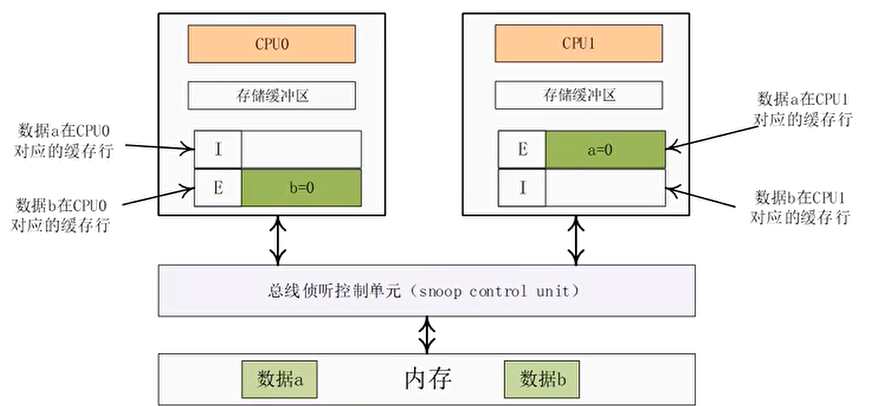
Data a has a cached copy in CPU1’s cache, and its state is E (Exclusive).
Data b has a cached copy in CPU0’s cache, and its state is E (Exclusive).
Then in a system with a store buffer, will an assert failure occur?
Time T1 CPU0 executes the statement “a=1”

At time T2 CPU0 executes the statement “b=1”

Time T3 CPU1 executes the statement “while(b==0)”

At time T4 CPU0 receives a bus read signal.
At time T5 CPU1 obtains the latest value of b

At time T6 assert failure

Flowchart of the entire process

Solution to the side effect: use a write memory barrier instruction
- Store bufferIt optimizes the performance degradation caused by long waits for acknowledgment signals between multi-core processors, but it still…There is no guarantee that the order of writes between multi-core CPUs is visible to other cores.
- Write memory barrier instructionFor example, smp_wmb() marks all writes in the current store buffer that have not yet been flushed to the cache, and thenflush the store buffer, ensuring that subsequent write operations can only be executed after these marked writes have been updated to the cache.

Solution: add a write memory barrier statement:

At time T1CPU0 executes the statement “a=1”

At time T2 CPU0 executes “smp_wmb()”

At time T3: CPU0 executes the statement “b=1”

At time T4 CPU1 executes the statement “while(b==0)”

At time T5

The state of data b on CPU0 changes from E to S
At time T6

At time T7

At time T8
CPU0 receives the response signal for data a and writes data a from the store buffer into the cache.

At time T9
Data b in the store buffer is also written into the cache.

Time T10

Time T11

Time T12

Because the smp_wmb() instruction is added between a=1 and b=1, the operation of writing b=1 to the cache must be executed after a=1 is written to the cache.
Optimization method 2: Invalidate Queue
- The store buffer in optimization method 1 is very small and can easily fill up.
- One reason for CPU stalling is:Waiting for other CPUs to perform the “invalidate” operation, which is relatively time-consuming.
- Invalidate queue:**Buffer the invalidate operation, first reply with an acknowledgment signal to the requester, and then slowly perform the invalidate operation.**so that other CPUs do not have to wait for a long time.
The CPU that replies to the invalidate operation does not need this data itself.
- When a CPU receives a bus request, if it needs to perform an operation to invalidate a local cache line, it adds the request to the invalidate queue and immediately replies with an acknowledgment signal to the other party, without needing to invalidate the cache line before responding.
- If a CPU adds a request to the invalidate queue, then before the invalidate operation corresponding to that request is completed, the CPU cannot send any bus messages related to the cache line corresponding to that request to the bus.

Side effects of the invalidate queue
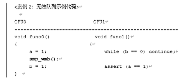
Assume the initial values of data a and data b are 0, data a has copies on both CPU0 and CPU1 with state S, and data b has a cache copy on CPU0 with state E. Will the assert succeed? (The answer is no, because the invalidate queue may cause CPU1 to delay processing the invalidate operation for a.)
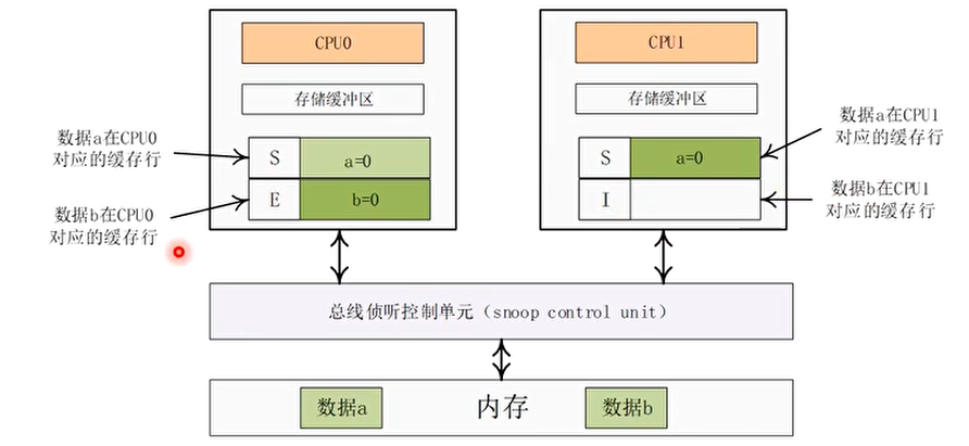
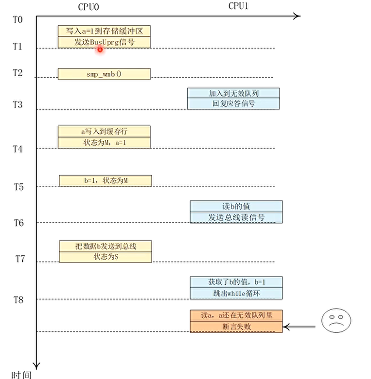
Solution to the side effect: use read memory barrier instructions
Read memory barrier instructionOKEnsure that all invalid operations in the invalid queue are completed before the read operations following the read barrier instruction can be executed.。

Summary of memory barriers and cache coherence.
In SMP, a simple load and store instruction is not simple; its behavior needs to be analyzed in conjunction with the MESI cache coherence protocol.
Memory barriers need to be analyzed in conjunction with MESI cache coherence.
Store buffers and invalid queues are hardware optimization techniques, but they also bring some side effects.
The read memory barrier instruction acts on the invalid queue, ensuring that after all pending invalid operations in the invalid queue are completed, subsequent read operations can be executed.
The write memory barrier instruction acts on the store buffer, ensuring that after the data in the store buffer is written to the cache, subsequent write operations can be executed.
Memory barrier APIs provided in the Linux kernel.
The Linux kernel abstracts a minimal set of common APIs that every processor architecture can support.

In-depth understanding of ARM64 memory barrier instructions.
