
Timeline
Timeline
2025-10-24
init
This article introduces the basic concepts and implementation mechanisms of ARM memory management. It first analyzes the disadvantages of directly using physical memory, such as insufficient protection of process address space, low memory utilization, and address relocation issues, thereby introducing the paging mechanism and virtual memory. The article explains in detail the mapping process from virtual addresses to physical addresses, including the disadvantages of single-level page tables and the advantages of multi-level page tables (such as two-level page tables). For the ARMv8 architecture, this article summarizes its page table format, including that AArch64 only supports Long Descriptor, three page sizes (4KB/16KB/64KB), a four-level page table structure (L0-L3), and descriptor types for block mapping and page mapping. In addition, it introduces the MMU hardware unit in VMSA, TTBR registers, the role of TLB, and the translation flow from VA to IPA to PA in virtualization scenarios. Finally, the article mentions the concept of shareability domain (Shareability) in page table attributes.
Reference documents:

Basic knowledge and concepts of memory management
Disadvantages of directly using physical memory
- Process address space protection issue. All user processes can access all physical memory, so malicious programs can modify the memory data of other programs.
- Low memory utilization. If the memory space required by the process about to run is insufficient, a process must be selected to be swapped out entirely. This mechanism causes a large amount of data to be swapped in and out, making efficiency very low.
- Program execution address relocation problem

Basic concepts of the paging mechanism
- Virtual Memory
- Virtual Address Space
- Physical Memory
- Page Frame
- Virtual Page Frame Number
- Physical Page Frame Number
- Page Table (PT)
- Page Table Entry (PTE)
The process of mapping virtual addresses to physical addresses

Single-level page table

Disadvantages of using a single-level page table
- The processor uses a single-level page table. The virtual address space is 32 bits wide, with an addressing range of 4GB. The physical address space is also 32 bits wide, supporting up to 4GB of physical memory. Additionally, the page size is 4KB. To map the entire 4GB address space, 4GB/4KB = 1MB page table entries are needed. Each page table entry occupies 4 bytes, so a total of 4MB of physical memory is required to store this page table.
- **Each process has its own set of page tables, and the page table base address needs to be switched during process switching.**As with the single-level page table mentioned above, each process needs to be allocated 4MB of contiguous physical memory to store its page table. This is unacceptable because it wastes too much memory.
- Multi-level page table: map level by level on demand, without mapping the entire address space at once.
Level 2 page table

VMSA
Virtual Memory System Architecture
- VMSA provides the MMU hardware unit
- Translation from virtual address to physical address
- Access permissions
- Memory attribute check
- The MMU hardware unit is used to implement VA to PA translation
- Hardware walks the page table (table walking)
- The TTBR register holds the base address of the page table
- The TLB stores the most recently used VA to PA translation results

Without virtualization, translation has only one stage, mapping VA to PA
In a virtualization scenario, translation needs to first convert to IPA

TTBR0_ELx Used for each process’s address space
TTBR1_ELx Used for kernel space, shared by all processes

Page tables in ARMv8
AArch64 only supports the Long Descriptor page table format
AArch32 supports two page table formats
- Armv7-A Short Descriptor format
- Armv7-A (LPAE) Long Descriptor format
AArch64 supports three different page sizes: 4KB, 16KB, 64KB
Larger page sizes can reduce the size of page tables
The address bus width supports 48 bits or 52 bits
52-bit width: ARMv8.2-LVA is implemented and the 64 KB translation granule
Taking 48-bit bus width as an example
The virtual address VA is divided into two spaces,Each space supports up to 256TB
- The lower virtual address space is from 0x0000_0000_0000_0000 to 0x0000_FFFF_FFFF_FFFF
- The upper virtual address space is from 0xFFFF_0000_0000_0000 to 0xFFFF_FFFF_FFFF_FFFF

Virtual address space partitioning (Fault is a non-canonical region, CPU cannot access)
Four-level page table

4-level page table
AArch64 page table descriptors
The following are all 48-bit virtual addresses, 4KB pages
Page table descriptors for L0~L2

Block typeIndicates that it describes a very large block of memory

L3 page table descriptor


| Level | Corresponds to Linux abstraction | Possible descriptor types |
|---|---|---|
| L0 (optional) | PGD | Table / Fault |
| L1 | PUD | Block (1GB, granule=4K) / Table / Fault |
| L2 | PMD | Block (2MB, granule=4K) / Table / Fault |
| L3 | PTE | Page (4KB, granule=4K) / Fault |
Note:
- Block entry Can only appear in the intermediate levels (L1/L2), indicating a large page mapping that maps a large physical address space, equivalent to the last-level page table.
- PTE (L3) Cannot be Block, only Page or Fault.
- The output address is that of the next-level page tablePA(i.e., physical address); if the current level is already the last level, it directly outputs the address of the physical page
Page table attributes
Only points to Final physical page (block/page) Only the entry of … needs page table attributes
ARM ARM D5.3.3Chapter
- bit[0] → Whether valid:
0= Invalid (Fault entry)1= Valid (Valid entry)
- bit[1] → Type (only meaningful when valid):
0= Block entry (block mapping, large page mapping)1= Table entry (points to the next-level page table; becomes a Page entry at the last level)
So the page table attributes of block and page are as follows:

High-order attributes and low-order attributes
Only describesBlockandPage


Share Domain
Non-shareable
This represents memory accessible only by a single processor or other agent, so memory accesses never need to be synchronized with other processors. This domain is not typically used in SMP systems.
Inner shareable
This represents a shareability domain that can be shared by multiple processors, but not necessarily all of the agents in the system. A system might have multiple Inner Shareable domains. An operation that affects one Inner Shareable domain does not affect other Inner Shareable domains in the system. An example of such a domain might be a quad-core Cortex-A57 cluster.
Outer shareable
An outer shareable (OSH) domain re-order is shared by multiple agents and can consist of one or more inner shareable domains. An operation that affects an outer shareable domain also implicitly affects all inner shareable domains inside it.
However, it does not otherwise behave as an inner shareable operation.
Full system
An operation on the full system (SY) affects all observers in the system.
Contiguous Block entries
- ARMv8 An optimization using TLB: usingone TLB entry to complete the VA-to-PA translation of multiple contiguous pages
- Conditions for using the Contiguous bit
- The VAs corresponding to the pages must be contiguous
- For 4KB pages, 16 contiguous pages
- For 16KB pages, 32 or 128 contiguous pages
- For 64KB pages, 32 contiguous pages
- Contiguous pages must have the same attributes
- The start address must be aligned with the size of the contiguous region
4KB page table
- 4-level page table
- 48-bit virtual address
- Each level of page table uses 9 bits for indexing (512 entries)

16KB page table
4-level page table
48-bit virtual address
L0 page table has only two entries
L1, L2, and L3 page tables use 11 bits for indexing (2048 entries)

64KB page table
- Level 3 page table
- 48-bit virtual address
- L1 page table has only 64 entries
- L2 and L3 page tables use 13 bits for indexing (8192 entries)

Two separate page table design
- User space (EL0) and kernel space (EL1) use a design with two separate page table base addresses
- When the high 16 bits of the virtual address are 1, TTBR1_EL1 is selected
- When the high 16 bits of the virtual address are 0, TTBR0_EL1 is selected

Address lookup example

In a simple address translation, only one level of lookup is involved. Suppose we use a 64KB granule and a 42-bit virtual address. The MMU maps the virtual address as follows:
- If VA[63:42] = 1, TTBR1 is used for the base address of the first-level page table. When VA[63:42] = 0, TTBR0 is used for the base address of the first-level page table.
- The page table contains 8192 64-bit page table entries and is indexed by VA[41:29]. The MMU reads the relevant level 2 page table entry from the table.
- The MMU checks the validity of the page table entry and whether the requested memory access is permitted. Assuming it is valid, the memory access is allowed.
- In Figure 12-7, the page table entry refers to a 512MB page (it is a block descriptor).
- Bit[47:29] is taken from the page table entry and forms Bit[47:29] of the physical address.
- Since we have a 512MB page, Bit[28:0] of the VA is taken as PA[28:0]. See page 12-15 for the effect of granule size on the translation table.
- The full PA[47:0] is returned, along with other information in the page table entry.

A 64KB granule and a 42-bit virtual address space are assumed.
- If VA[63:42] = 1, TTBR1 is used for the base address of the first-level page table. When VA[63:42] = 0, TTBR0 is used for the base address of the first-level page table.
- The page table contains 8192 64-bit page table entries and is indexed by VA[41:29]. The MMU reads the relevant level 2 page table entry from the table.
- The MMU checks the validity of the level 2 page table entry and whether the requested memory access is permitted. Assuming it is valid, the memory access is allowed.
- In Figure 12-8, the level 2 page table entry points to the address of the level 3 page table (it is a table descriptor).
- Bit[47:16] is taken from the level 2 page table entry to form the base address of the level 3 page table.
- Bit[28:16] of the VA is used to index the level 3 page table entry. The MMU reads the relevant level 3 page table entry from the table.
- The MMU checks the validity of the level 3 page table entry and whether the requested memory access is permitted. Assuming it is valid, the memory access is allowed.
- In Figure 12-8, the level 3 page table entry refers to a 64KB page (it is a page descriptor).
- Bit[47:16] is taken from the level 3 page table entry to form PA[47:16].
- Since we have a 64KB page, VA[15:0] is taken as PA[15:0].
- The full PA[47:0] is returned, along with other information in the page table entry.
System registers related to page tables
TCR_EL1
Translation Control Register
Configure address space size and page table granule

Configure address space size and page table granule

- IPS: Intermediate Physical Address Size, used to configure the physical address size. For example, 48 bits corresponds to a maximum physical space of 256 TB.
- TG1andTG0: Configure the page table granularity size, e.g., 4KB, 16KB, 64KB.
- T1SZ: Used to configure the size that the TTBR1_EL1 page table can manage. The calculation formula is 2^(64-T1SZ) bytes.
- T0SZ: Used to configure the size that the TTBR0_EL1 page table can manage. The calculation formula is 2^(64-T0SZ) bytes.
In ARM64, the upper bits of a virtual address are not used arbitrarily; they are constrained by TCR_EL1.T0SZ / T1SZ restrictions.
Cache-related fields

- SH1: Set memory-related cache attributes. These memories are accessed through the TTBR1_EL1 page table. For example, Non-shareable, Outer Shareable, Inner Shareable.
- SH0: Set memory-related cache attributes. These memories are accessed through the TTBR0_EL1 page table.


- ORGN1: Set attributes related to Outer Shareable.
- ORGN0: Set attributes related to Outer Shareable.
- IRGN1: Set attributes related to Inner Shareable.
- IRGN0: Set attributes related to Inner Shareable.

TCR_In EL1, the SH0/SH1, IRGN0/IRGN1, ORGN0/ORGN1 fields are only used for memory accesses that do not undergo address translation (i.e., when the MMU is disabled), or serve as “default” attributes in certain special contexts. Once the MMU is enabled, memory attributes are completely determined by the page table entries + MAIR_EL1 determines.
SCTLR_EL1
System Control Register (EL1)

- M: Enable/disable MMU
- I: Enable/disable instruction cache
- C: Enable/disable data cache
TTBR0_EL1
Points to the base address of the TTBR0 page table, typically used for EL1/EL0 page table mappings.

TTBR1_EL1
Points to the base address of the TTBR1 page table, typically used for EL1/EL0 page table mappings.

MAIR_EL1
Memory Attribute Indirection Register


ARM architecture designers believe:In the vast majority of systems, 8 memory types are sufficient to cover all usage scenarios.
123456789101112 | // Typical MAIR configuration in the Linux kernel// Write to MAIR_EL1 registerasm volatile("msr mair_el1, %0" :: "r" (MAIR_EL1_SET)); |
ID_AA64MMFR0_EL1
AArch64 Memory Model Feature Register 0, reports the processor’s support for support for page tables, address ranges, and memory features


| field | bit | meaning |
|---|---|---|
| PARANGE | [3:0] | Supported physical address width |
| ASID | [7:4] | Supported ASID (Address Space ID) width in bits |
| BIGENDEL | [11:8] | Supports EL1/EL0 large page extension |
| SNSMEM | [15:12] | Whether secure memory access is supported |
| BIGENDEL0 | [19:16] | Supports EL0 large page extension |
| TGRAN16 | [23:20] | Supports 16KB pages |
| TGRAN64 | [27:24] | Supports 64KB pages |
| TGRAN4 | [31:28] | Supports 4KB pages |
CPACR_EL1
Architectural Feature Access Control Register


FPEN field (CPACR_EL1[21:20])
FPEN = Floating-point Enable controls, controls whether EL0/EL1 accesses to SVE, Advanced SIMD, and floating-point registers are trapped by EL1/EL2。
- Register effects:
- AArch64:
- FPCR、FPSR
- SIMD/Floating-point registers
V0-V31(including D0-D31 / S0-S31 views)
- AArch32 / Advanced SIMD:
- FPSCR
- Q0-Q15 (including D0-D31 / S0-S31 views)
- AArch64:
- Exception reporting:
- EL0/EL1 trap → EC syndrome =
0x07 - EL2 trap → EC syndrome =
0x00(when EL2 is enabled andHCR_EL2.TGE = 1)
- EL0/EL1 trap → EC syndrome =
| FPEN | Behavior description |
|---|---|
| 0b00 | Instructions at both EL0 and EL1 are trapped, unless CPACR_EL1.ZEN has already trapped them |
| 0b01 | Only EL0 instructions are trapped, EL1 is not trapped |
| 0b10 | Instructions at both EL0 and EL1 are trapped(same as 0b00) |
| 0b11 | No instructions are trapped(registers are freely accessible) |
In simple terms:
FPEN controls whether user mode (EL0) or kernel mode (EL1) can directly use the floating-point/SIMD/SVE registers, usually configured before enabling the MMU
Together with CPACR_EL1.ZEN, it provides fine-grained control over accesses at different levels.
Common configurations:
0b11 → Not trapped, allowing all EL0/EL1 instructions to access FP/SIMD.
0b00/0b10 → Trapped, typically used in security or virtualization scenarios.

MDSCR_EL1


TDCC
TDCC = 0 → User mode EL0 can directly read/write the DCC registers.
TDCC = 1 → EL0 accesses to DCC registers are trapped to EL1/EL2, often used for security/virtualization/debug control。
DCC is Debug Communication Channel, it provides a data transfer interface between the CPU and the debugger (Debug Host), only when TDCC=0 can JTAG be used to access DCC registers

Enabling the MMU
12345678910111213141516171819202122232425262728293031323334353637383940414243444546474849505152535455565758596061 | // enable_mmu.S// AArch64 assembly: setting TTBR0/TTBR1, TCR_EL1 and enable MMU (SCTLR_EL1.M = 1)// Convention:// Input registers:// X0 = TTBR0 base (physical address of level-translation table for TTBR0)// X1 = TTBR1 base (physical address of level-translation table for TTBR1)// X2 = TCR_EL1 value to program (caller constructs an appropriate value)// Returns: no return value; executes ISB after enabling MMU.//// Usage example: prepare X0/X1/X2 in C code, then jump to this routine or call it with inline assembly. 4 enable_mmu_el1 .type enable_mmu_el1, %// For readability, some comments are placed near instructions; see each line's comment for details.enable_mmu_el1: // 1) Write page table base address to TTBR0/TTBR1 // TTBR0_EL1 is used for the lower address space (VA range controlled by T0SZ) // TTBR1_EL1 is used for the higher address space (VA range controlled by T1SZ) // X0/X1 must contain the page table base address (aligned), usually physical address >> translation_granule_shift MSR TTBR0_EL1, X0 // TTBR0_EL1 <- X0 MSR TTBR1_EL1, X1 // TTBR1_EL1 <- X1 // 2) Write TCR_EL1 (Translation Control Register) // X2 must be constructed by the caller as an appropriate TCR value (e.g., 4KB granule, 48-bit VA, etc.). // TCR controls: T0SZ/T1SZ (VA width), TG0/TG1 (granule), IRGN/ORGN/SH and other memory attributes. MSR TCR_EL1, X2 // TCR_EL1 <- X2 // 3) ISB — ensure the just-written TTBR/TCR are visible to the instruction stream before subsequently enabling the MMU // ISB ensures that the effects of previous system register writes take effect before subsequent instructions (synchronizes the context). ISB // (Optional/Recommended) Invalidate all TLB entries before enabling the MMU. // This is useful when there are stale translations, but when enabling the MMU for the first time and the page tables are newly constructed, it can be performed selectively depending on the platform. // TLBI VMALLE1 // invalidate all translations for EL1 stage1 by VA/ASID (virtualization-related) // MRS X3, CNTVCT_EL0 // TLBI VMALLE1 // DSB SY // ISB // 4) Read SCTLR_EL1 (System Control Register) MRS X3, SCTLR_EL1 // X3 = current SCTLR_EL1 // 5) Set the M bit (bit 0) of SCTLR_EL1 to enable the MMU // Additionally: other bits usually need to be set/checked at the same time, e.g., C (data cache enable), I (instruction cache enable), // SA/SP/EE and other bits are adjusted as required by the platform. Here only the MMU is enabled (M=1). // If the caller also wants to enable caches, it should set the C/I bits here or before. ORR X3, X3, #1 // X3 = X3 | 0x1 -> set M bit // 6) Write back SCTLR_EL1 MSR SCTLR_EL1, X3 // SCTLR_EL1 <- X3 // 7) ISB — ensure the MMU configuration and register changes take effect immediately for subsequently executed instructions ISB RET .size enable_mmu_el1, .-enable_mmu_el1 |
TBI(Top Byte Ignore)
The TBI (Top Byte Ignore) feature in the ARMv8-A architecture, also calledTop byte ignore, it allows you toThe highest 8 bits of the virtual address ([63:56]) are used to store extra information without affecting memory access. This mechanism is also called Tagged Pointers, a feature provided by ARM to programming languages and runtime systems.
Under normal circumstances, the address must be valid
In 64-bit systems, registers are 64-bit, but virtual addresses are not fully 64-bit — ARMv8 typically supports 48-bit or 52-bit virtual addresses. So the virtual addressThe top 16 bits must be sign-extended:
| Virtual address type | The high 16 bits must be |
|---|---|
| user-mode memory | 0x0000 |
| kernel high addresses | 0xFFFF |
If you write[63:48]it as any other value, the CPU will triggerAddress size fault。
Before Enabling TBI in TCR_EL1 after (withTBI0andTBI1controlling respectively), the CPU will ignore the highest 8 bits of the address[63:56], meaning you can write arbitrary tag data to these 8 bits tostore additional information without affecting memory access!
Note: The kernel/user address is still determined by VA[55]; 1 indicates a kernel address, 0 indicates a user address space.
BeforeTCR_EL1There are two fields:
TBI0→ Control When EL0 accesses using TTBR0 address whether to enable pointer tagsTBI1→ Control When EL1 accesses using TTBR1 address whether to enable pointer tags
Memory attributes
Memory attributes defined by ARMv8
ARMv8 architecture processors provide two memory attributes
Normal Memory
Normal memory is weakly ordered, with no other additional constraints, providing the highest memory access performance
Device Memory
Processor access to device memory has many restrictions, such as no speculative access, etc. Device memory is executed strictly in instruction order. The ARMv8 architecture defines multiple device memory attributes.
- Device-nGnRnE (does not support gathering, does not support instruction reordering, does not support early write acknowledgment)
- Device-nGnRE (does not support gathering, does not support instruction reordering, supports early write acknowledgment)
- Device-nGRE (does not support gathering, supports instruction reordering, supports early write acknowledgment)
- Device-GRE (supports gathering, supports instruction reordering, supports early write acknowledgment)
Gathering or non Gathering (G or nG)
This attribute determines whether it is possible tomerge multiple accesses into a single bus transaction to this memory region。
- If an address is marked as non-gathering (nG), thenthe number and size of accesses performed to that location on the memory bus must exactly match the number and size of explicit accesses in the code。
- If an address is marked as Gathering (G), the processor canfor example, merge two byte writes into a single halfword write. For regions marked as Gathering, it can alsomerge multiple memory accesses to the same memory location。
For example, if the program reads the same location twice, the core only needs to perform one read, and can return the same result for both instructions. For reads from a region marked as non-Gathering, the data value must come from the endpoint device. It must not be snooped from the write buffer or other locations.
Re-ordering (R or nR)
This determineswhether accesses to the same device can be reordered with respect to each other。If an address is marked as non-reordering (nR), accesses within the same block always appear on the bus in program order. The size of this block is implementation-defined (IMPLEMENTATION DEFINED). If the size of this block is large, it can span several table entries. In this case, the ordering rules are observed for any other accesses also marked as nR.
Early Write Acknowledgement (E or nE)
This determineswhether an intermediate write buffer between the processor and the slave device being accessed is allowed to send a write completion acknowledgment. In modern SoCs (System-on-Chip), processors (such as CPUs) access peripherals or memory through an interconnect. To improve performance, the interconnect typically includeswrite buffer (Write Buffer), used to temporarily store data that has not yet been actually written to the target device.
But in some scenarios,it must be ensured that the data has actually reached the target device before the write operation is considered complete(for example, writing to a register triggers a hardware action), while in other scenarios it is possible toacknowledge the write completion earlyto improve throughput (for example, writing to normal memory).
This leads to E (Early) and nE (not Early) the difference between.
If an address is marked as non-early write acknowledgment (nE), the write response must come from the peripheral, i.e.,prohibitedearly acknowledgment. The write completion signalmust be issued by the target peripheral itself, i.e., the dataafter it is actually received by the peripheral, only then is the processor notified that the write operation is complete.
If the address is marked for Early Write Acknowledgement (E), thenallows buffers in the interconnect logic to issue a write acceptance signal before the endpoint device actually receives the write.. This is essentially information to the external memory system that allows the write buffers in the interconnect towhen the data has not yet actually reached the target peripheralsend a “write complete” acknowledgement signal to the processor.
Defined in the Linux kernel
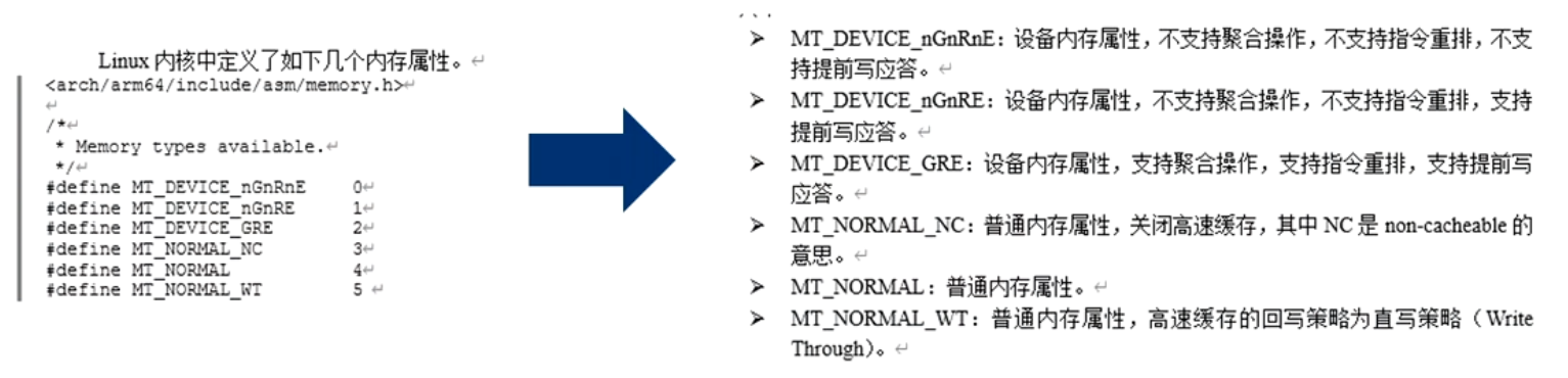
Memory attributes are not stored in the page table entries, but are stored inMAIR_ELnregisters (Memory Attribute Indirection Register)。
There is a 3-bit index value (AttrInx[2:0]) in the page table entry to look up the MAIR_ELn register。

Memory attributes defined in the Linux kernel
- The operating system (Linux) defines a series of attributes based on the memory attributes defined by ARMv8 and the read/write properties of memory.
- PAGE_KERNEL: the most ordinary memory page
- PAGE_KERNEL_RO: ordinary memory page that is read-only in the kernel
- PAGE_KERNEL_ROX: ordinary page that is read-only and executable in the kernel
- PAGE_KERNEL_EXEC: ordinary page executable in the kernel
- PAGE_KERNEL_EXEC_CONT: ordinary page executable in the kernel, and is multiple physically contiguous pages

Example of creating page tables in Linux 5.0
- Global directory entry PGD (Page Global Directory) corresponds to the L0 page table of arm64
- Upper directory entry PUD (Page Upper Directory) corresponds to the L1 page table of arm64
- Middle directory entry PMD (Page Middle Directory) corresponds to the L2 page table of arm64
- Page table entry (Page Table Entry) corresponds to the L3 page table of arm64
arch/arm64/mm/mmu.c


- Find the PGD table entry by address addr

- Find the end address of the range covered by the corresponding PGD using addr

- Set the PGD page table entry

- Find the PUD table entry by address addr

Experiment
Experiment 1: Establish identity mapping

ARM64 uses 4-level page table(PGD → PUD → PMD → PTE), each level uses 9-bit index(512 entries), page size is 4KB:
| Level | Name | Index bits | Mapping range | Number of entries | Table size |
|---|---|---|---|---|---|
| L0 | PGD | [47:39] | 512 GB | 512 | 4KB |
| L1 | PUD | [38:30] | 1 GB | 512 | 4KB |
| L2 | PMD | [29:21] | 2 MB | 512 | 4KB |
| L3 | PTE | [20:12] | 4 KB | 512 | 4KB |
Note: If a page table entry at a certain level is marked as SECTION (block mapping), then skip the next level and directly map a large block of memory.


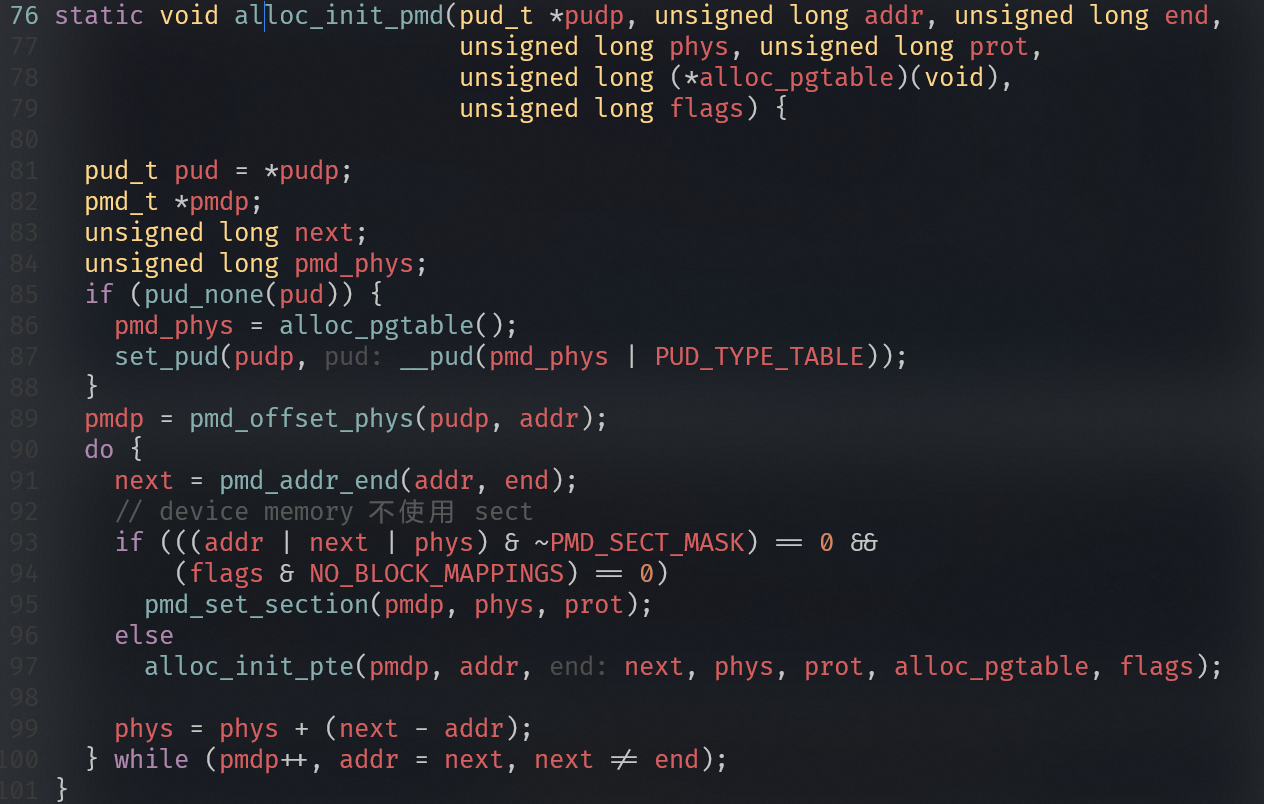


Why use identity mapping?
To avoid problems when enabling the MMU:
- When the MMU is disabled, all addresses accessed by the processor are physical addresses.When the MMU is enabled, the addresses accessed by the processor become virtual addresses.
- Modern processors aremulti-stage pipeline architecture.,The processor prefetches multiple instructions into the pipeline in advance.When the MMU is enabled, the processor has already prefetched multiple instructions, and these instructions are prefetched using physical addresses. When the instruction that enables the MMU completes execution, the MMU function takes effect. Therefore, this is toensure the processor can continuously fetch instructions before and after enabling the MMU.。
Experiment 2: Why the MMU doesn’t run.

Obviously,_text_boot to _the memory attribute of etext should be mapped as PAGE_KERNEL_ROX
From_etext to TOTAL_MEMORY is what should be mapped as PAGE_KERNEL
Experiment 3: Implement an MMU page table dump feature.

Experiment 4: System crash caused by modifying page attributes.

Xiaoming did this experiment. In the text section of the linker script, he allocated a 4KB read-only page, then implemented a walk_pgtable() function to traverse the page table and find the corresponding PTE, and found that no matter how he set it, he couldn’t make the page writable.
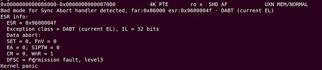


The problem is here.

should be changed to

Experiment 5: Verify the ldxr and stxr instructions.


The reason is that we did not set the sharable attribute.


Experiment 6: Address Translation AT Instruction


Reading the MMU Chip Manual
TODO